Characterizing order in organic and inorganic semiconductors - PowerPoint PPT Presentation
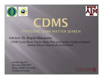
Characterizing order in organic and inorganic semiconductors Paulette Clancy Cornell University KDI Order Team NSF Review June 2002 Cornell Engineering Knowledge and Distributed Intelligence Group Cornell Engineering Knowledge and Distributed
Characterizing order in organic and inorganic semiconductors Paulette Clancy Cornell University KDI Order Team NSF Review June 2002 Cornell Engineering Knowledge and Distributed Intelligence Group Cornell Engineering Knowledge and Distributed Intelligence Group
Overview of the presentation • Cornell KDI Order Team • Focus and scientific objectives • Computational tools • Scientific advances in order-related topics • Necessity for a team approach • Summary of current status • Recommendations to NSF Cornell Engineering Knowledge and Distributed Intelligence Group Cornell Engineering Knowledge and Distributed Intelligence Group
Team Members Faculty • Paulette Clancy Chem. and Biomolec. Engr. HARD Fernando Escobedo Chem. and Biomolec. Engr. SOFT Edwin Kan Electrical and Computer Eng. HARD George Malliaras Materials Sci. and Engr. SOFT Michael P. Teter Physics HARD Michael O. Thompson Matls. Sci. and Engr. HARD Grad Students • Six PhD students; 3 departments; 50% women and minorities Aleksandra Chojnacka* MSE Devashish Choudhary CBE Leonard Harris* CBE Chungho Lee ECE Chin Lung Kuo CBE Ritesh Shetty CBE Michelle Swiggers* MSE * Denotes women or minority students Undergraduate Researchers • 25 students over 3 yrs; 50% women and minorities Visitors • David Dunlap (UNM, Alb.) SOFT External Affiliates • Lawrence Livermore National La., IBM Corp; Intel Corp., Kodak Corp. Cornell Engineering Knowledge and Distributed Intelligence Group Cornell Engineering Knowledge and Distributed Intelligence Group
Group Focus and Objectives Focus : Explore the relationship between order and properties (structural, electrical, mechanical) Scientific Objectives : • Develop a coherent language for the expression of order (semantic and mathematical) • Develop computational tools to express this language and to create partially ordered systems • Understand and manipulate order-property relationships at interfaces (e.g. metal/Si; organic/metal; organic/Si) 0 1 Order Gas Liquid Glass Amorphous Crystal Cornell Engineering Knowledge and Distributed Intelligence Group Cornell Engineering Knowledge and Distributed Intelligence Group
Challenges • Ambiguous terminology of order in semiconductors • Despite much work on simulating amorphous Si, no convincing best way to create a realistic description. • Separate families of empirical intermolecular models : one for hard and one for soft materials. • Scale of organic semiconductors a challenge for electronic structure (ES) packages. • Multiscale calculations reveal that the accuracy of ES needs to be higher. Cornell Engineering Knowledge and Distributed Intelligence Group Cornell Engineering Knowledge and Distributed Intelligence Group
Initial Project Objectives • How do we create a- Si (or a- Ge) models that can be used in dynamical simulations? [MC and MD routes] • How well does virtual a -Si resemble real a- Si? • Is a- Si a unique phase ? • Can we create an electronic structure code with LDA accuracy but tight-binding speed ? • How does charge transport occur in organic semiconductors? • How is this mediated by the presence of an interface ? • How does this knowledge translate into working electronic devices ? Creation → → → → Characterization → → → → Knowledge → → → → Application Cornell Engineering Knowledge and Distributed Intelligence Group Cornell Engineering Knowledge and Distributed Intelligence Group
Scope, work plan, and inter-relationships in the project Develop “Signature Create + Characterize Understand a-Ge → c-Ge a -Si, a -Ge Cell” order parameter transformation as (PC) CA (FE) CT exemplified in explosive crystallization (MOT,PC) CA E Develop Virtual Nature of order-disorder Charge Gibbs ensemble MC (locally/globally) in hard Transport in code for solids CT semiconductors dissimilar (FE) systems I I Create + Characterize metal nanodots on Si (ECK,PC) Develop faster and Understand charge CA E more efficient ab transport in hard/soft initio tool heterosystems CT (MPT) I (All) Enhance charge Use existing ab initio transport in tools Create + Characterize pentacene / Si systems ITR : Arias + DFT++ pentacene / Si interfaces (GM) EPSRC : Gillian/Bowler E (KMC, MD, statics) UK CONQUEST (FE,PC) CT CA Key to symbols CT E Computational tool Experiments CA I Computational analysis Information Cornell Engineering Knowledge and Distributed Intelligence Group Cornell Engineering Knowledge and Distributed Intelligence Group
Meta-project”: Pentacene/Si systems In-situ X-ray characterization of Electrical hard/soft interfaces New ab initio code characterization of metal nanodots on (MOT) E pentacene (MPT, PC) CT (ECK) E Understand charge transport in hard/soft hetero systems Characterization of charge Compare to existing transport in pentacene/X codes: DFT++ & (and other organic Creation and CONQUEST semiconductor/X) characterization of systems order and charge CT (GM) E transport in pentacene/Si systems (FE, PC) CA Key to symbols CT E Computational tool Experiments CA Computational analysis I Information Cornell Engineering Knowledge and Distributed Intelligence Group Cornell Engineering Knowledge and Distributed Intelligence Group
Computational Tools • “Signature Cell” method to determine order on a local or global scale. Richer in information than traditional schemes = Configuration Potential = Signature exact match at Pseudo-potential global minimum σ 2 σ σ σ 0 U(r) Phase space σ σ 1 σ σ -1 r • New electronic structure code (Harris-like formalism but with “tunable” accuracy (at the expense of computational efficiency) Cornell Engineering Knowledge and Distributed Intelligence Group Cornell Engineering Knowledge and Distributed Intelligence Group
Signature Cell Method (Illustration) Superimpose signature Perform MC moves Rotation moves Breathing moves Parallel tempering swaps Find best match = Configuration atoms = Signature atoms Cornell Engineering Knowledge and Distributed Intelligence Group Cornell Engineering Knowledge and Distributed Intelligence Group
Computational Tools irtual Gibbs ensemble MC method. Allows MC simulation of liquid-solid Particle transfer attempt transitions Box II Box I Faked Move on a box Volume transfer attempt 4.45 ccelerated MD schema in a new arena. Transformations of bulk solids; 4.4 Molecular Dynamics Evolution of a quenched liquid Silicon Self-Guided MD 4.35 kinetics . Co-ordination no Hyper MD using various MD schemes: Hyper MD 4.3 and Self Guided MD 4.25 4.2 (Stillinger Weber potential, 4.15 Isothermal Isobaric simultaion) 4.1 4.05 0 1 2 3 4 5 6 Computational Timesteps ( 1 0 6 )
Information about order-property relations • Created a new route to a-Si and a-Ge. Accelerated MD makes ‘quench and anneal’ viable. • Evidence for a-Si as a unique phase; prediction of the structural lifetime of (as yet undiscovered) glassy Si. • Created an order map for post-explosively crystallized Ge T end = 826 K 800 columnar morphology (high-temperature plateau ) (film too thin or substrate temperature too low) T min , T columnar , T end [K] K µ µ µ µ m 750 4 2 1 h -1 + y K no explosive crystallization g 6 4 o 6 = l o h T columnar p r o Morphology diagram m 700 l a K n o m for Germanium i t µ µ µ µ i s n 6 a 2 r 3 t 650 r 1 - o h d + e p K o l l 7 a c 7 s 4 = 600 n i T m 550 0.4 0.6 0.8 1.0 -1 [ µ m -1 ] -1 -1 h x h end h Cornell Engineering Knowledge and Distributed Intelligence Group Cornell Engineering Knowledge and Distributed Intelligence Group
Explosive Crystallization (Illustration) Steady state conditions: V o T cl > T al v cl = v al V o ~ 1/R sample t=0 time R sample V batt laser amorphous liquid crystalline Cr
Information about order-property relations continued… • Surprising evidence for the width of the mediating liquid layer in explosive crystallization and its implications for modeling . • Demonstrated that alignment in pentacene films can be induced by surface alignment layers used in liquid crystals, leading to pronounced increase on transport properties Charge transport in organic-inorganic junction Pentacene-Silicon interface Cornell Engineering Knowledge and Distributed Intelligence Group Cornell Engineering Knowledge and Distributed Intelligence Group
Information about order-property relations continued… • Use physical and electrical methods to characterize self assembly of metal nano-crystals on semiconductors and insulators. Collaboration with ab-initio calculation to build realistic models. • Demonstrate improved nonvolatile memory device characteristics by using metal nanocrystals • Demonstrate new carrier injection schemes 2 to 3 orders of magnitude better than conventional contact schemes by using metal nanocrystal interfaces Nano-crystal growth of Au on SiO 2 CMOS Device Cornell Engineering Knowledge and Distributed Intelligence Group Cornell Engineering Knowledge and Distributed Intelligence Group
Recommend
More recommend
Explore More Topics
Stay informed with curated content and fresh updates.

