Carbon-Based Electronics: Will there be a carbon age to follow the - PowerPoint PPT Presentation
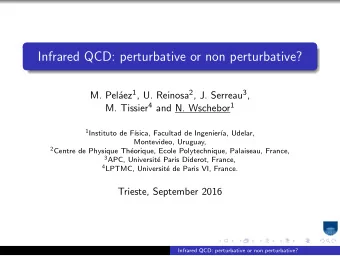
Carbon-Based Electronics: Will there be a carbon age to follow the silicon age? Jeffrey Bokor EECS Department UC Berkeley jbokor@eecs.berkeley.edu Solid State Seminar 9-13-13 1 Outline Review of development of Carbon Nanotube (CNT)
Carbon-Based Electronics: Will there be a carbon age to follow the silicon age? Jeffrey Bokor EECS Department UC Berkeley jbokor@eecs.berkeley.edu Solid State Seminar 9-13-13 1
Outline • Review of development of Carbon Nanotube (CNT) transistors (for logic) – Issues, progress, prospects • Advent of graphene – Recognition of promise of graphene nanoribbons (GNRs) for logic transistors – Issues, progress, prospects • Summary of prospects for carbon transistors 2
3 C60: Birth of carbon Nanotech era
Main properties of carbon nanotubes predicted before discovery! semiconductor Applied Physics Letters metal 4
Single-wall carbon nanotubes discovered in carbon ‘soot’ by TEM Iijima and Ichihashi, Nature (1993) [NEC] 5
CNT Transistor Laser vaporization method for CNT synthesis Tans, et al., Nature (1998) [Dekker group, Delft] 6
Catalytic CVD growth of CNTs on a surface Catalyst: Fe(NO3)3 ⋅ 9H2O/alumina/methanol suspension CVD at 1000C with methane Kong, et al, Nature (1998) [Dai group, Stanford] 7
Self-Aligned Ballistic FETs w/High-k 0.2 V V DS = -0.1,-0.2,-0.3 V -5 10 d~1.7 nm -5 L ~ 50 nm -0.1 V -6 10 I DS ( A) -10 -I DS (A) -7 10 -0.4 V -15 -8 10 -0.7 V -20 -9 -1.0 V 10 -1.3 V -25 -0.4 -0.3 -0.2 -0.1 0.0 -1.5 -1.0 -0.5 0.0 0.5 V DS (V) V G (V) • Pd zero-barrier height contact • > 5 mA/um at V g = V DS =0.4V Javey, et al, Nano Lett. (2004) [Dai group, Stanford] 8
High Performance p- and n-FETS • Doping by adsorption • Lg = 80nm Javey, et al, Nano Lett. (2005) [Dai group, Stanford] 9
CNT-CMOS Integration Chip NMOS binary tree 11-bit decoder 2048 back-gated CNT transistors >4000 Si NMOS transistors, 1 m Microlab baseline process Tseng, et al, Nano Lett. (2004) [UCB/Stanford, Bokor/Dai groups] 10
Carbon Nanotube + Silicon MOS Integrated Circuit I on 1x10 -5 10 -6 Id (A) Total: 523 devices 150 10 -7 Semiconducting 10 -8 I min nanotubes only 100 -15 -10 -5 0 5 10 15 Vgs (V) counts 209 Devices 50 Tseng, et al, Nano Lett. (2004) [UCB/Stanford, Bokor/Dai groups] 0 0 1 2 3 4 5 6 7 Log (on/off) 11
Direct correlation to diameter variation 1 tube per device Ion, Vgs-Vt=-7v 1x10 -6 1x10 -7 1x10 -5 1x10 -8 Ion (A) Imin (A) 1x10 -9 1x10 -10 10 -6 Measurement Limit 10 -11 10 -12 0.5 1.0 1.5 2.0 2.5 3.0 3.5 4.0 0.5 1.0 1.5 2.0 2.5 3.0 3.5 4.0 Diameter (nm) Diameter (nm) d=2.9nm d=2.2nm 1x10 -5 d=1.1nm 1x10 -6 Tseng, et al, Nano Lett. (2006) 1x10 -7 [UCB, Bokor group] Id (A) 1x10 -8 1x10 -9 1x10 -10 10 -11 -15 -10 -5 0 5 10 15 Vgs (V) 12
Parallel Tube CNTs • To get large drive, need to stack multiple tubes in parallel with common contacts, gate • Do parallel array currents add? • How close can tubes be stacked? • Important for ultimate circuit application 13
Parallel Array of Self-Aligned Ballistic FETs -4 10 G D -6 -I DS (A) 10 -8 10 V DS = -0.1,-0.2,-0.3 V S -10 10 -1 0 1 V G (V) S G -50 D I DS ( A) -100 G -150 S V GS = -0.9 to 0.3 V SWNT S in 0.2 V steps -200 G -0.6 -0.4 -0.2 0.0 D V DS (V) Javey, et al., 1 st demonstration of a parallel array Nano Lett. (2004) • [Stanford, Dai group] • ~200 uA of current for the array of 8 tubes. 14
CNT Array Density Limited by Screening Wang, et al. SISPAD (2003) [IBM] 15
CNT Array Transistor Circuit Performance Jie, et al., ISSSC (2007) [Stanford/USC, Wong/Mitra/Zhou groups] 16
Vision for CNT channel array MOSFETs CNTs CNTs or or SNWs SNWs S S Metal Metal D D Gate Gate HfO 2 HfO 2 pitch pitch L g L g L gc L gc Gate Dielectric k 1 Gate Dielectric k 1 Bulk Dielectric k 2 Bulk Dielectric k 2 Substrate Substrate • Array of 1D channels, densely packed • Density 200-250 per m • No metallic tubes • Narrow diameter distribution 17
A Multiple Growth Strategy to High Densities • Single-crystal quartz growth substrate • “Epitaxial” CNT growth Hong, et al, Adv. Mat. (2010) • Layer transfer to Si wafer [UIUC, Rogers group] 18
Density Scaling by Multiple Transfers Removal of m-tubes by ‘breakdown’ as grown: 15/um transferred: 15/um 2X transfer: 29/um 4X transfer: 55/um Wang, et al., Nano Res. (2010) [USC, Chou group] 19
Selective Removal of m-tubess From Aligned Arrays Coat with small Induce Joule heating O 2 plasma Remove film and molecule film selectively in m ‐ SWNTs etch exposed electrodes; build to form trenches by m ‐ SWNTs circuits on thermocapillarity remaining s ‐ SWNTs M S M S M S M S S S S S SiO 2 SiO 2 SiO 2 SiO 2 Si (p ++ ) Si (p ++ ) Si (p ++ ) Si (p ++ ) J. Rogers group, UIUC 20
Dynamics of Thermocapillary Flow Joule Heating by a SWNT ( ∆ T~5-15C) Heating options: • Gated electrical Joule heating • Selective laser absorption • Selective microwave absorption Jin, et al., Nat. Nano. (2013) [UIUC, Rogers group] t= 0 0.1 1 10 100 300 s 2 m 21
Solution phase nanotube ‘sorting’/purification “Density gradient” centrifugation Arnold, et al., Nat. Nano. (2006) [Northwestern, Hersam group] 22
Electrical results on sorted CNTs Percolating network transistor Sorted tube transistor high on/off ratio Arnold, et al., Nat. Nano. (2006) [Northwestern, Hersam group] 23
DNA sequence specific wrapping for sorting “size exclusion” chromatography Tu, et al., Nature (2009) [Dupont, Zheng group] 24
Purified Single Chirality (10,5) SWNTs (10,5) Separated SWNTs (10,5) 200nm Starting HiPco material Zhang, et al, JACS (2009), [Stanford/Dupont, Dai/Zheng groups] DNA used: (TTTA)3T 25
FETS with 99% Semiconducting Tubes Mostly (10,5) SWNTs Purely Percentage(%) 40 S semiconducting 30 Mixed 20 100nm 10 D 0 < 2 2-4 4-6 > 6 lo g ( I o n /I o ff ) -5 Average 15 tubes per 10 -6 10 device -7 10 Ion/Ioff >10 2 : 88% -8 10 semiconducting -I ds (A) -9 10 -10 tubes: 10 99% (0.99 15 ~ 88%) -11 10 1000mV -12 10 500mV 100mV -13 10 10mV -14 10 Zhang, et al, JACS (2009), -2 -1 0 1 2 V gs (V) [Stanford/Dupont, Dai/Zheng groups] 26
Solution phase array assembly by Langmuir- Blodgett technique Li, et al. JACS (2007) [Stanford, Dai group] ~70/um ~80/um 27
Solution processed CNTs are as good as CVD tubes at nanoscale Lg CVD tubes Franklin and Chen, Nat. Nano. (2010) [IBM Choi, et al., ACS Nano (2013) [UCB, Bokor/Javey groups] 28
Ultimate scaling study M. Luisier (Purdue) Also DG AGNR SG AGNR GAA CNT GAA NW DG UTB 29
Simulation parameters and assumptions Device Characteristics: - All: L g =5nm, V DD =0.5 V, EOT=0.64nm (3.3nm of HfO 2 with ε R =20) - SG and DG AGNR: width=2.2nm, normalization by width - GAA CNT: diameter=1.58, 1.0, and 0.6 nm, normalization by diameter GAA and -NW: Si, diameter=3nm, transport=<110>, 1% uniaxial strain - - DG UTB: Si, body=3nm,, transport=<110>, 1% uniaxial strain Simulation Approach: - Same quantum transport simulator for all devices based on Non-equilibrium Green’s Functions (NEGF) formalism with atomistic resolution of simulation domain and finite element method for Poisson equation Bandstructure model: single-p z for carbon and sp 3 d 5 s * for silicon (tight-binding) - - Ballistic limit of transport (no electron-phonon scattering nor interface roughness taken into account) - Intrinsic device performances (no contact series resistances included) - No gate leakage currents included - No structure optimization for any of the selected devices 30
I d -V gs at V ds =0.5V in carbon-based Devices AGNR width: 2.2nm / CNT diameter: 1.58nm / Band Gap E g =0.56 eV HfO 2 SiO 2 EOT=0.64nm EOT=0.64nm • Same EOT gives very different electrostatic gate-channel coupling M. Luisier (Purdue) 31
Gate Dielectric Effect In Carbon-Based Devices Comparison of Conduction Band Edge and Spectral Current in Single-Gate AGNR with 0.64nm SiO 2 ( ε R =3.9) and 3.3nm HfO 2 ( ε R =20) => same EOT=0.64nm OFF- state SiO 2 HfO 2 • Effective channel length is longer for the thicker HfO 2 • Barrier widens and tunneling current drops 32
Extreme (sub-10 nm S-D Tunneling regime) d=1.58 nm CNT FETs Transfer Characteristics Sub-threshold swing 3.3nm HfO 2 EOT=0.64nm V ds =0.5V V ds =0.5V d=1.58 nm 5nm ≤ L g ≤ 12nm • Bandgap 0.56 eV GAA- CNT (d=1.58 nm) scales poorly M. Luisier, et al., IEDM (2011) [Purdue/MIT/UCB, Lundstrom/Antoniadis/Bokor groups] 33
Gate-length trend for 1 nm CNTs Transfer Characteristics Sub-threshold Slope • Bandgap 0.8 eV GAA- CNT (d=1.0 nm) scales better M. Luisier, et al., IEDM (2011) [Purdue/MIT/UCB, Lundstrom/Antoniadis/Bokor groups] 34
Gate-length trend for 0.6 nm CNTs I d -V gs at V ds =0.5V in CNT FETs with d=0.6nm and 5 ≤ L g ≤ 12 nm Transfer Characteristics Sub-threshold Slope • Bandgap 1.4 eV GAA- CNT (d=0.6 nm) scales well M. Luisier, et al., IEDM (2011) [Purdue/MIT/UCB, Lundstrom/Antoniadis/Bokor groups] 35
Comparison of different channel materials I d -V gs at V ds =0.5V in CNT, NW, and UTB Devices 3.3nm HfO 2 , EOT=0.64nm • CNT with d=0.6nm and NW with d=3nm have same band gap E g =1.4eV • CNT with d=1.0nm has band gap E g =0.817eV • Bandgap 0.8 eV GAA-CNT (d=1.0 nm) scales poorly • Bandgap 1.4 eV GAA-CNT (d=0.6 nm) scales well • Si NW (d=3 nm) scales very well due to high-mass and band-gap 36
Recommend
More recommend
Explore More Topics
Stay informed with curated content and fresh updates.
