Bias-Stress Instability in GaN Field-Effect Transistors Jess A. del - PowerPoint PPT Presentation
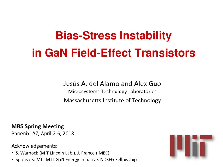
Bias-Stress Instability in GaN Field-Effect Transistors Jess A. del Alamo and Alex Guo Microsystems Technology Laboratories Massachusetts Institute of Technology MRS Spring Meeting Phoenix, AZ, April 2-6, 2018 Acknowledgements: S.
Bias-Stress Instability in GaN Field-Effect Transistors Jesús A. del Alamo and Alex Guo Microsystems Technology Laboratories Massachusetts Institute of Technology MRS Spring Meeting Phoenix, AZ, April 2-6, 2018 Acknowledgements: • S. Warnock (MIT Lincoln Lab.), J. Franco (IMEC) • Sponsors: MIT-MTL GaN Energy Initiative, NDSEG Fellowship
Application space for future power electronics Important role for GaN power electronics in future 2
Favored structure: GaN MIS-HEMT • MIS-HEMT: Metal-Insulator-Semiconductor High Electron Mobility Transistor 2DEG • High-mobility 2DEG at AlGaN/GaN interface • Dielectric to suppress gate leakage current and increase gate swing • On Si for low cost 3
Main concern with GaN MIS-HEMTs: reliability and stability • Si substrate defects in GaN • Multiple interfaces, many trapping sites • Uncertain electric field distribution across gate stack 4
Bias-Temperature Instability (BTI) Device stability during operation: key concern, particularly V T Al 2 O 3 /AlGaN/GaN SiN/AlGaN/GaN HfO 2 /AlGaN/GaN Lagger, IEDM 2012 Zhang, SST 2014 Winzer, PSSa 2016 5
BTI in GaN MOSFETs Simpler than MIS-HEMTs: single GaN/oxide interface • Industrial prototype devices Guo, IRPS 2015 Guo, IRPS 2016 • Gate dielectric: SiO 2 /Al 2 O 3 (EOT=40 nm) Guo, TED 2017 6
Experimental methodology Constant-V GS , stress-interrupt experiments at RT: Guo, TED 2017 1. Device initialization through thermal detrapping step Minor impact: Δ V T < 20 mV, Δ S < 30 mV/dec 2. Stress and characterization: measure V T , peak g m , S at V DS =0.1 V After 50 characterization runs: Δ V T < 10 mV, Δ g m < 0.02 mS/mm, Δ S < 15 mV/dec 3. Recovery phase with terminals grounded and periodic characterization 4. Final thermal detrapping 7
Threshold voltage evolution • PBTI: V GS,stress >0 Δ V T >0 Guo, TED 2017 • NBTI: V GS,stress <0 Δ V T <0 • | Δ V T | increases with stress voltage and time • Fully recoverable no defect generation 8
Transconductance evolution • PBTI: V GS,stress >0 g m,max ↓ Guo, TED 2017 • NBTI: V GS,stress <0 g m,max ↑ • | Δ g m | increases with stress voltage and time • Fully recoverable no defect generation 9
Subthreshold swing evolution Guo, TED 2017 • PBTI: V GS,stress >0 S unchanged • NBTI: V GS,stress <0 S unchanged • No interface state generation 10
Correlation between Δ V T and Δ g m PBTI PBTI NBTI NBTI Guo, TED 2017 • Good correlation between PBTI and NBTI during stress and recovery • One physical mechanism, fully reversible 11
Functional dependence of V T V T well described by power-law function : PBTI NBTI NBTI PBTI Guo, TED 2017 Consistent with electron trapping/detrapping in oxide 12
PBTI/NBTI: Recoverable electron trapping/detrapping in oxide 0 13
PBTI/NBTI: Recoverable electron trapping/detrapping in oxide 0 14
PBTI/NBTI: Recoverable electron trapping/detrapping in oxide 0 15
PBTI/NBTI: Recoverable electron trapping/detrapping in oxide 0 16
PBTI/NBTI: Recoverable electron trapping/detrapping in oxide 0 17
PBTI in HfO 2 /InGaAs system 0 Cai, IEDM 2016 18
Oxide trapping in other high-k/MOS systems Al 2 O 3 /Si Al 2 O 3 /InGaAs HfO 2 /Ge Wu, IEDM 2005 HfO 2 /Si 0 Al 2 O 3 /InGaAs Si HK/MG Franco, IRPS 2014 Zafar, TDMR 2005 Franco, IEDM 2017 19
Oxide trapping in other high-k/MOS systems Al 2 O 3 /Si Al 2 O 3 /InGaAs HfO 2 /Ge Wu, IEDM 2005 HfO 2 /Si 0 Al 2 O 3 /InGaAs Si HK/MG Franco, IRPS 2014 Zafar, TDMR 2005 Franco, IEDM 2017 20
Oxide trapping in other high-k/MOS systems Al 2 O 3 /Si Al 2 O 3 /InGaAs HfO 2 /Ge Wu, IEDM 2005 HfO 2 /Si 0 Al 2 O 3 /InGaAs Si HK/MG Franco, IRPS 2014 Zafar, TDMR 2005 Franco, IEDM 2017 21
Oxide trapping in other high-k/MOS systems Al 2 O 3 /Si Al 2 O 3 /InGaAs HfO 2 /Ge Wu, IEDM 2005 HfO 2 /Si 0 Al 2 O 3 /InGaAs Si HK/MG Franco, IRPS 2014 Zafar, TDMR 2005 Franco, IEDM 2017 22
Oxide trapping in other high-k/MOS systems Al 2 O 3 /Si Al 2 O 3 /InGaAs HfO 2 /Ge Wu, IEDM 2005 HfO 2 /Si 0 Al 2 O 3 /InGaAs Si HK/MG Franco, IRPS 2014 Zafar, TDMR 2005 Franco, IEDM 2017 23
What are these defects? Prime suspect: O vacancies Al 2 O 3 /GaN band alignment: Formation energy of O vacancies: 0 Liu, APL 2010 Defect states in Al 2 O 3 right above conduction band edge of GaN 24
What are these defects? Prime suspect: O vacancies Al 2 O 3 /GaN band alignment: Formation energy of O vacancies: 0 Liu, APL 2010 Defect states smear into bands in amorphous material 25
How to mitigate? Look at CMOS literature t IL ↑ AC BTI more benign Krishnan, IRPS 2012 Reduce high-k thickness Introduce SiON interfacial Cartier, IEDM 2011 layer Cartier, IEDM 2011 0 Short, high-T anneal Reduce I G LaSiO interlayer Franco, IRPS 2017 Krishnan, IRPS 2012 Franco, IRPS 2017 26
How to mitigate? Look at CMOS literature t IL ↑ AC BTI more benign Krishnan, IRPS 2012 Reduce high-k thickness Introduce SiON interfacial Cartier, IEDM 2011 layer Cartier, IEDM 2011 0 Short, high-T anneal Reduce I G LaSiO interlayer Franco, IRPS 2017 Krishnan, IRPS 2012 Franco, IRPS 2017 27
How to mitigate? Look at CMOS literature t IL ↑ AC BTI more benign Krishnan, IRPS 2012 Reduce high-k thickness Introduce SiON interfacial Cartier, IEDM 2011 layer Cartier, IEDM 2011 0 Short, high-T anneal Reduce I G LaSiO interlayer Franco, IRPS 2017 Krishnan, IRPS 2012 Franco, IRPS 2017 28
How to mitigate? Look at CMOS literature t IL ↑ AC BTI more benign Krishnan, IRPS 2012 Reduce high-k thickness Introduce SiON interfacial Cartier, IEDM 2011 layer Cartier, IEDM 2011 0 Short, high-T anneal Reduce I G LaSiO interlayer Franco, IRPS 2017 Krishnan, IRPS 2012 Franco, IRPS 2017 29
How to mitigate? Look at CMOS literature t IL ↑ AC BTI more benign Krishnan, IRPS 2012 Reduce high-k thickness Introduce SiON interfacial Cartier, IEDM 2011 layer Cartier, IEDM 2011 0 Short, high-T anneal Reduce I G LaSiO interlayer Franco, IRPS 2017 Krishnan, IRPS 2012 Franco, IRPS 2017 30
How to mitigate? Look at CMOS literature t IL ↑ AC BTI more benign Krishnan, IRPS 2012 Reduce high-k thickness Introduce SiON interfacial Cartier, IEDM 2011 layer Cartier, IEDM 2011 0 Short, high-T anneal Reduce I G LaSiO interlayer Franco, IRPS 2017 Krishnan, IRPS 2012 Franco, IRPS 2017 31
How to mitigate? Look at CMOS literature t IL ↑ AC BTI more benign Krishnan, IRPS 2012 Reduce high-k thickness Introduce SiON interfacial Cartier, IEDM 2011 layer Cartier, IEDM 2011 0 Short, high-T anneal Reduce I G LaSiO interlayer Franco, IRPS 2017 Krishnan, IRPS 2012 Franco, IRPS 2017 32
How to mitigate? Look at CMOS literature t IL ↑ AC BTI more benign Krishnan, IRPS 2012 Reduce high-k thickness Introduce SiON interfacial Cartier, IEDM 2011 layer Cartier, IEDM 2011 0 Short, high-T anneal Reduce I G LaSiO interlayer Franco, IRPS 2017 Krishnan, IRPS 2012 Franco, IRPS 2017 33
NBTI under harsher stress High-voltage and high-temperature stress: Guo, IRPS 2016 • Three regimes: N egative ∆V T positive ∆V T negative ∆V T • Permanent negative ∆V T after final thermal detrapping 34
NBTI under harsher stress High-voltage and high-temperature stress: Trapping in GaN channel under gate edge (recoverable) Guo, IRPS 2016 • Three regimes: N egative ∆V T positive ∆V T negative ∆V T • Permanent negative ∆V T after final thermal detrapping 35
NBTI under harsher stress High-voltage and high-temperature stress: Trapping in GaN channel under gate edge (recoverable) Interface trap formation (permanent) Guo, IRPS 2016 • Three regimes: N egative ∆V T positive ∆V T negative ∆V T • Permanent negative ∆V T after final thermal detrapping 36
Conclusions • PBTI and NBTI (benign stress): ‒ recoverable ΔV T , Δ g m due to electron trapping/detrapping in pre- existing oxide traps ‒ Experimental observations well described by oxide trapping model • Many avenues for mitigation study Si high-k/MOS literature • New degradation physics under harsher stress (NBTI): ‒ r ecoverable ΔV T >0, ΔS due to electron trapping in substrate ‒ non- recoverable ΔV T <0, Δ g m , Δ S due to interface state formation 37
Recommend
More recommend
Explore More Topics
Stay informed with curated content and fresh updates.
