Negative-Bias Temperature Instability (NBTI) of GaN MOSFETs Alex - PowerPoint PPT Presentation
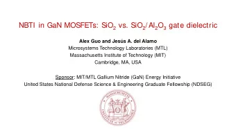
Negative-Bias Temperature Instability (NBTI) of GaN MOSFETs Alex Guo and Jess A. del Alamo Microsystems Technology Laboratories (MTL) Massachusetts Institute of Technology (MIT) Cambridge, MA, USA Sponsor: MIT/MTL Gallium Nitride (GaN)
Negative-Bias Temperature Instability (NBTI) of GaN MOSFETs Alex Guo and Jesús A. del Alamo Microsystems Technology Laboratories (MTL) Massachusetts Institute of Technology (MIT) Cambridge, MA, USA Sponsor: MIT/MTL Gallium Nitride (GaN) Energy Initiative United States National Defense Science & Engineering Graduate Fellowship (NDSEG) 1
Purpose To understand the physics of and to mitigate NBTI in GaN n-MOSFETs. 2
Outline 1. Motivation 2. Experimental setup 3. Three regimes of NBTI 4. Summary of contributions 3
Outline 1. Motivation 2. Experimental setup 3. Three regimes of NBTI 4. Summary of contributions 4
GaN for power electronics • Promising for a wide range of applications 30 V 600 V > 1200 V 5
GaN for power electronics • Promising for a wide range of applications 30 V 600 V > 1200 V • Negative-Bias Temperature Instability (NBTI) is a major concern: • Operational instability • Long-term reliability 6
GaN for power electronics • Promising for a wide range of applications 30 V 600 V > 1200 V • Negative-Bias Temperature Instability (NBTI) is a major concern: • Operational instability • Long-term reliability Challenge: mechanisms responsible for NBTI? 7
GaN MIS-HEMT for high voltage applications • MIS-HEMT: Metal-Insulator-Semiconductor High Electron Mobility Transistor • Large gate swing, low gate leakage Passivation Passivation 8
GaN MIS-HEMT for high voltage applications • MIS-HEMT: Metal-Insulator-Semiconductor High Electron Mobility Transistor • Large gate swing, low gate leakage Passivation Passivation [Lagger, TED 2014] • Presence of gate oxide brings new stability and reliability concerns not present in HEMTs 9
NBTI of GaN MIS-HEMT Stress Recovery V GS,stress = -10 V [Meneghini, EDL 2016] Large ∆V T < 0 at moderate V GS,stress , slow partial recovery • Possible mechanism: trapping in multiple layers and interfaces • 10
NBTI of GaN MIS-HEMT Stress Recovery V GS,stress = -10 V [Meneghini, EDL 2016] Large ∆V T < 0 at moderate V GS,stress , slow partial recovery • Possible mechanism: trapping in multiple layers and interfaces • To better understand NBTI: Stress voltage dependence ; dynamics of S and g m,max ; simpler structure 11
Simpler GaN MOSFET structure • Industrial prototype devices • SiO 2 /Al 2 O 3 composite gate dielectric, EOT = 40 nm oxide GaN channel metal • Isolate oxide and oxide/GaN interface IRPS 2015: PBTI This work: physical mechanisms behind NBTI of GaN MOSFET 12
Outline 1. Motivation 2. Experimental setup 3. Three regimes of NBTI 4. Summary of contributions 13
Experiment flow and FOM definition Device screening and initialization Stress and characterization Recovery and characterization Thermal detrapping • V T : V GS value when I D = 1 µA/mm • S : Extracted at I D = 0.1 µA/mm I/V sweep • g m,max : Extracted from I DS -V GS ramp • All at V DS = 0.1 V Increase stress voltage • First sample: ~ 1- 2 s after removal or temperature of stress 14
Outline 1. Motivation 2. Experimental setup 3. Three regimes of NBTI 4. Summary of contributions 15
V T shift overview This work: GaN MOSFET After TD *TD: Thermal Detrapping Three regimes: Small negative ∆V T p ositive ∆V T negative ∆V T • Permanent negative ∆V T after TD • 16
V T shift overview This work: GaN MOSFET Si HKMG p-MOSFET t HfO 2 = 2.5 nm After TD *TD: Thermal Detrapping [Zafar, TDMR 2005] Three regimes: Small negative ∆V T p ositive ∆V T negative ∆V T • Permanent negative ∆V T after TD • 17
Regime 1 (low-stress) Time evolution of ΔV T and ΔS at RT After TD After TD • Negative Δ V T ,| Δ V T | increases with t stress and |V GS,stress | • Minimal ∆S • Complete recovery 18
Regime 1 (low-stress) I D -V GS and C G -V G characteristics V GS,stress = -1 V, t stress = 10,000, RT • Simple parallel V T shift that completely recovers 19
Regime 1 (low-stress) Temperature dependence • Rate of V T shift shows slight positive T dependence 20
Regime 1 (low-stress) Modeling • Power law with n = 0.28 to 0.4 • Similar to PBTI observation [Guo, IRPS 2015] 21
Regime 1 (low-stress) Δ V T mechanism Consistent with electron detrapping and retrapping from/to pre- • existing oxide traps Initial Electron detrapping Electron retrapping Also seen in Si HKMG MOSFETs [Young, IRWS 2003] and Al 2 O 3 /InGaAs • MOSFETs [Wrachien, EDL 2011] 22
Regime 2 (mid-stress) t stress evolution of Δ V T , Δ S and Δ g m,max at RT ∆V T > 0 • |V GS,stress |↑ , t stress ↑ Δ V T ↑, ΔS ↑, |Δ g m,max | ↑ • ∆ V T , ∆S and | Δ g m,max | mostly recoverable • 23
Regime 2 (mid-stress) Temperature dependence V GS,stress = -10 V • All parameter shifts enhanced by T • At high T, recovery incomplete transition to regime 3 24
Regime 2 (mid-stress) ∆V T and ∆S correlation • ΔV T and ΔS are linearly correlated throughout the entire experiment, and completely recover 25
Regime 2 (mid-stress) C-V characteristics V GS,stress = -20 V, t stress = 1,000 s, RT Temporary charge buildup • Temporary charge buildup around threshold after stress 26
Regime 2 (mid-stress) ∆V T mechanism [Jin, IEDM 2013] 27
Regime 2 (mid-stress) ∆V T mechanism y x [Jin, IEDM 2013] • High field at edges of gate Zener trapping in GaN substrate • Energy bands at surface of GaN channel ↑ Positive Δ V T , Δ S • Thermal process effective in electron detrapping 28
Regime 3 (high-stress) t stress evolution of Δ V T at RT Similar to regime 2 Additional permanent negative Δ V T 29
Regime 3 (high-stress) t stress evolution of Δ V T at RT • t stress ↑, |V GS,stress | ↑ permanent | Δ V T |↑, ΔS ↑ and |Δ g m,max |↑ 30
Regime 3 (high-stress) Temperature dependence V GS,stress = -70 V, t stress = 1 – 10,000 s • T ↑ permanent | Δ V T |↑, ΔS ↑ and |Δ g m,max |↑ 31
Regime 3 (high-stress) Correlation of permanent Δ V T , Δ S and Δ g m,max Measurements at RT • Permanent ΔV T , ΔS and Δg m,max well correlated 32
Regime 3 (high-stress) I D -V GS and C G -V G characteristics V GS,stress = -70 V, t stress = 500 s, T = 125 ° C • Prominent Δ V T , Δ S and Δ g m,max correlate with a softening of C-V characteristics around threshold 33
Regime 3 (high-stress) ∆V T Mechanism • Interface state generation under high gate stress • Well-studied mechanism in Si MOS system [Schroder, JAP 2007] 34
Outline 1. Motivation 2. Experimental setup 3. Three regimes of NBTI 4. Summary of contributions 35
NBTI of GaN MOSFETs Identified three degradation mechanisms: Regime 1 (low-stress) • Observation: small, recoverable negative ∆V T • Mechanism: electron detrapping from pre-existing oxide traps • Regime 2 (mid-stress): • Observation: recoverable positive ∆V T and ∆S • Mechanism: Zener trapping in channel under edges of gate • Regime 3 (high-stress): • Observation: negative, non-recoverable ∆V T , ∆ S and ∆ g m,max • Mechanism: interface state generation • 36
Recommend
More recommend
Explore More Topics
Stay informed with curated content and fresh updates.
