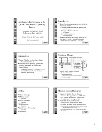
Analog/Digital Control Methods Instructor: Fionn Sheerin, Senior - PowerPoint PPT Presentation
Analog and Hybrid Analog/Digital Control Methods Instructor: Fionn Sheerin, Senior Product Marketing Engineer, Microchip Technology, Inc. HOUSEKEEPING Housekeeping Presentation Text Chat Questions and Answers Wrap-up Agenda
Analog and Hybrid Analog/Digital Control Methods Instructor: Fionn Sheerin, Senior Product Marketing Engineer, Microchip Technology, Inc.
HOUSEKEEPING • Housekeeping • Presentation • Text Chat Questions and Answers • Wrap-up
Agenda Analog Control System and control loop operation Voltage and current mode control methods Design and circuit example Hybrid Analog / Digital Control Digital management of analog control loops Track 3: Full Digital System Control 3
SMPS Loop Closure Why “close the loop”? Feedback control determines the performance of the SMPC in terms of line regulation, load regulation, and dynamic response Better control 4
Switching Regulators Switching regulators monitor the input voltage, output voltage, switch or inductor current in order to adjust the switch duty cycle in response to line and load changes + Vin Synchronous Buck Vout Circuit Control - + Vin Asynchronous Vout Control Boost Circuit - 5
Control Loops 6
Analog SMPC Loop Closure v 1 V O L 1 V S V S + R LOAD Q 1 D 1 C 1 v 1 V O 0 Buck converter I O i L 0 V S -V O V O v L 0 i S I S 0 DT D 2 T T T 7
Analog SMPC Loop Closure v 1 V O L 1 V S V S + R LOAD Q 1 D 1 C 1 v 1 V O 0 Buck converter I O i L v 1 V O L 1 0 V S + R LOAD Q 1 C 1 V S -V O V O v L 0 Switch conducting (DT) i S I S 0 DT D 2 T T T 8
Analog SMPC Loop Closure v 1 V O L 1 V S V S + R LOAD Q 1 D 1 C 1 v 1 V O 0 Buck converter I O i L v 1 V O L 1 0 V S + R LOAD Q 1 C 1 V S -V O V O v L 0 Switch conducting (DT) v 1 V O i S I S L 1 V S + R LOAD 0 D 1 C 1 DT D 2 T T T Diode conducting (D 2 T) 9
Analog SMPC Loop Closure v 1 V O L 1 V S V S + R LOAD Q 1 D 1 C 1 v 1 V O 0 Buck converter I O i L v 1 V O L 1 0 V S + R LOAD Q 1 C 1 V S -V O V O v L 0 Switch conducting (DT) v 1 V O i S I S L 1 V S + R LOAD 0 D 1 C 1 DT D 2 T T T Diode conducting (D 2 T) 10
Analog SMPC Loop Closure Input Output System 11
Analog SMPC Loop Closure Input Output System Error Feedback Reference 12
Analog SMPC Loop Closure Input Output System Error Feedforward Feedback Reference 13
Analog SMPC Loop Closure e Inputs u G u r G u u r Output Reference 14
Analog SMPC Loop Closure e u G 1 Inputs u GH r G u u r Output Reference If G is much bigger than one (large open loop gain) H u 1 Negative Feedback u H r 15
Analog SMPC Loop Closure PowerSystem e Power u Input Circuitry Output d Control Control Circuitry Feedback Feedforward u r Reference 16
Analog SMPC Loop Closure V S V O K PWR K LC K FB Control + K EA or K MOD Reference K EA(S) Error Amplifier with compensation K MOD Pulse width modulator K PWR Power switching topology K LC(S) Output power filter K FB Feedback T(s) = K EA(S) * K MOD * K PWR * K LC(S) * K FB Open-loop gain 17
SMPS Control Methods Voltage mode control Output voltage feedback into transfer function to adjust duty cycle Voltage mode control with feedforward Output and input voltages feed into transfer function to adjust duty cycle Current mode control Inductor current and output voltage feed into transfer function to adjust duty cycle 18
SMPS Control Methods v 1 V O V S V S + v 1 D V O 0 V RAMP PWM V C Comp K FB 0 + - - V C K EA V REF + D 0 DT DIRECT DUTY CYCLE CONTROL T T (VOLTAGE MODE CONTROL) 19
SMPS Control Methods v 1 V O V S V S + v 1 D V O 0 V RAMP PWM V C Comp K FB 0 + - - V C K EA V REF + D 0 DT DIRECT DUTY CYCLE CONTROL T T (VOLTAGE MODE CONTROL) 20
SMPS Control Methods v 1 V O V S V S + v 1 V O D 0 V C i S 0 Clock PWM S K FB Comp 0 + - D1 V C - Q K EA V REF + 0 DT T T PEAK CURRENT MODE CONTROL 21
Waveforms of Subharmonic Instability Stable Subharmonic operation instability V C V C I S I S i L i L m 1 m 2 0 0 Clock Clock S S 0 0 D D 0 0 DT DT T T T T 22
Adding Stabilizing Ramp v 1 V O V S + D Q Clock R S PWM K FB Comp + - V C - K EA V REF + 23
SMPS Control Methods Voltage Mode Current Mode Single feedback loop Two feedback loops Good noise immunity Poor noise immunity Good cross regulation for Good line response and multiple outputs gain constant Poor dynamic response Load regulation worse Error amplifier must Single pole account for double pole Inherent pulse-by-pulse LC in CCM (complex current limiting conjugate poles) Requires slope Loop gain varies with compensation (ramp) input voltage 24
SMPC Loop Closure Loop Design Procedure Define the control loop strategy and plot the tentative goal Plot the known part of the loop Bode plot of K MOD * K PWR * K LC(S) * K FB Define the crossover frequency Design and plot the error amplifier compensation network 25
Error Amplifier Compensation Example Buck - Continuous Inductor Current - Direct Duty Cycle Control L V O V Ramp Voltage V S V C + D CR C R Time DC Analysis V V V V C C O RAMP D V V D V V O S S C V V V RAMP RAMP S 26
Error Amplifier Compensation Example Buck - Continuous Inductor Current - Direct Duty Cycle Control L V O V Ramp Voltage V S V C + D CR C R Time DC Analysis V V V V C C O RAMP D V V D V V O S S C V V V RAMP RAMP S Control to Output Transfer Function v V 1 s O S Z ( ) ( ) H s H s e e 2 v V 1 ( s ) Q ( s ) C RAMP O O 1 1 R Q O Z R C L LC ESR O 27
Error Amplifier Compensation Example Buck - Continuous Inductor Current - Direct Duty Cycle Control L V O Design Example f 500 kHz T 2 S V S + S D CR C R V 10 V to 20 V S V 5 V I 1 A to 5 A O O R 5 to 1 D 0 . 5 to 0 . 25 L 15 H C 15 F R 100 m ESR V 2 . 5 V RAMP 28
Error Amplifier Compensation Example Buck - Continuous Inductor Current - Direct Duty Cycle Control L V O Design Example f 500 kHz T 2 S V S + S D CR C R V 10 V to 20 V S V 5 V I 1 A to 5 A O O Calculate System Poles and Zeros R 5 to 1 1 f 10 . 6 kHz D 0 . 5 to 0 . 25 O 2 LC L 15 H 1 f 106 kHz Z 2 R C C 15 F ESR R 100 m ESR V 2 . 5 V RAMP 29
Error Amplifier Compensation Example Buck - Continuous Inductor Current - Direct Duty Cycle Control L V O Design Example f 500 kHz T 2 S V S + S D CR C R V 10 V to 20 V S V 5 V I 1 A to 5 A O O Calculate System Poles and Zeros R 5 to 1 1 f 10 . 6 kHz D 0 . 5 to 0 . 25 O 2 LC L 15 H 1 f 106 kHz Z 2 R C C 15 F ESR Calculate Low Frequency Gain R 100 m ESR v v V V 8 ( 18 dB ) at 20 V O C S RAMP V 2 . 5 V 4 ( 12 ) at 10 RAMP dB V 30
Error Amplifier Compensation Example Buck - Continuous Inductor Current - Direct Duty Cycle Control f f 4 500 kHz 4 125 kHz Crossover Frequency Goal: C S E/A Gain Needed at Crossover: 18 40 log( f f ) 20 log( f f ) 23 . 4 dB Z O C Z Two second order filter poles at f o are compensated by two zeros at f o /2. This provides additional phase shift at f o for sudden second order transition. f f 2 10 . 6 kHz 2 5 . 3 kHz Z O ESR zero is compensated by a pole at least a decade above the two zeros. f P 53 kHz 31
Error Amplifier Compensation Example 60 Blue – Uncompensated Transfer Function 50 Red – Compensation Network Green – Final System 40 30 Gain (dB) 20 10 0 -10 -20 -30 0.1 1 10 100 1000 Frequency (kHz) 32
Error Amplifier Compensation Example V O C3 C1 R2 C2 R11 PWM Comp - V C K FB K EA - D R1 + R12 V REF + Pulse width modulator and Error amplifier Feedback gains Three Poles and Two Zeros w Z1 = 1 / (C1 * R1) K MOD = d / v C = 1 / V RAMP w Z2 = 1 / (C2 * R2) K MODX = d / v C = D / V RAMP w P0 = 0 = V O / (V S * V RAMP ) w P1 = 1 / (C1 * (R1 || R11) K FB = V O / V REF w P2 = 1 / (R2 * (C2 || C3) = R12 / (R11 + R12) 33
PWM Controller System Example V IN = 5-30V MCP19035 VIN BOOT 5V, LDO 25mA HIGHDR V OUT SHDN PHASE PWRGD LOWDR COMP FB GND 34
PWM Controller System Example V IN = 5-30V MCP19035 VIN BOOT 5V, LDO 25mA HIGHDR V OUT SHDN PHASE PWRGD LOWDR COMP FB Analog GND Compensation Network 35
Hybrid Analog / Digital Methods 36
Summary Discrete DC-DC implementations require loop closure, adding substantial design complexity compared to integrated solutions Same as integrated solutions: good regulator selection, passive component selection, and layout are required Digital features can be implemented in an analog control system Highest efficiency, highest performance systems require digital control Track 3: Digital Power Control 37
Recommend
More recommend
Explore More Topics
Stay informed with curated content and fresh updates.
