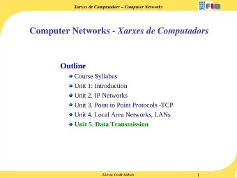
Unit 2 Digital Circuits (Logic) Moving from voltages to 1's and 0's - PowerPoint PPT Presentation
2.1 2.2 Unit 2 Digital Circuits (Logic) Moving from voltages to 1's and 0's ANALOG VS. DIGITAL 2.3 2.4 Signal Types Signals and Meaning Analog signal Analog Digital Continuous time signal where each voltage level has a unique
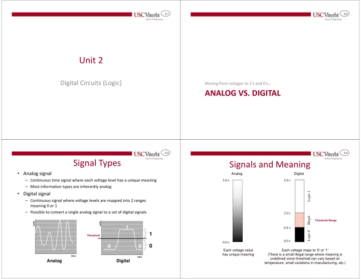
2.1 2.2 Unit 2 Digital Circuits (Logic) Moving from voltages to 1's and 0's… ANALOG VS. DIGITAL 2.3 2.4 Signal Types Signals and Meaning • Analog signal Analog Digital – Continuous time signal where each voltage level has a unique meaning 5.0 V 5.0 V – Most information types are inherently analog Logic 1 • Digital signal – Continuous signal where voltage levels are mapped into 2 ranges meaning 0 or 1 – Possible to convert a single analog signal to a set of digital signals 2.0 V Illegal Threshold Range volts volts 1 0.8 V Logic 0 1 Threshold 0.0 V 0.0 V 0 0 0 Each voltage value Each voltage maps to '0' or '1' has unique meaning (There is a small illegal range where meaning is time time undefined since threshold can vary based on Analog Digital temperature, small variations in manufacturing, etc.)
2.5 2.6 Analog vs. Digital USC students used to program analog computers! A Brief History COMPUTERS AND SWITCHING TECHNOLOGY 2.7 2.8 Transistor Overview Moore's Law & Transistors • Electronic computers require some kind Gate of "__________" (on/off) technology that +5V • We continue to shrink the size of the transistor structure allows one signal to turn another signal Source Drain controls the operation Voltage at the gate - - on or off Transistor • Moore's Law = Number of transistors able to be of the transistor is 'on' – Initially that was the ______________ but - - - - fabricated on a chip will _______________________ Silicon then replaced by the transistor High voltage at gate allows • Invented by Bell Labs in 1948 _________________________________ current to flow from source to drain • Uses ______________ materials (silicon) – We are approaching the physical limitations of this shrinking • Much smaller, faster, more reliable Gate – ______ compound annual growth rate over 50 years (doesn't burn out), and dissipated less 0V Transistor Source Drain power than previous technologies (e.g. is 'off' • No other technology has grown so fast so long - vacuum tubes). - • Transistors are the fundamental building block of Silicon computer HW Low voltage at gate prevents current from flowing from source to drain – Switching devices: Can conduct [on = 1] or not-conduct [off = 0] based on an input voltage Individual Transistors (About the size of your fingertip)
2.9 2.10 How Does a Transistor Work NMOS Transistor Physics • Let's review what we saw in the video… • Transistor inner workings • Transistor is started by implanting two n-type silicon – http://www.youtube.com/watch?v=IcrBqCFLHIY areas, separated by p-type n-type silicon (extra negative charges) - Source Drain Input Input - - - + + + p-type silicon ("extra" positive charges) 2.11 2.12 NMOS Transistor Physics NMOS Transistor Physics • A thin, insulator layer (silicon dioxide or just "oxide") • A thin, insulator layer (silicon dioxide or just "oxide") is placed over the silicon between source and drain is placed over the silicon between source and drain • Conductive polysilicon material is layered over the oxide to form the gate input Gate Input Source Input Drain Output Source Input Drain Output conductive - - polysilicon - - - - - - + + Insulator Layer + Insulator Layer + + n-type silicon (extra + n-type silicon (extra (oxide) (oxide) negative charges) negative charges) p-type silicon p-type silicon ("extra" positive charges) ("extra" positive charges)
2.13 2.14 NMOS Transistor Physics NMOS Transistor Physics • Positive voltage • Electrons can flow (charge) at the gate through the Gate Input Gate Input input repels the negative channel Source Input + Drain Output Source Input + Drain Output extra positive + from the source + + n-type + n-type - charges in the p- + input to the drain + - + + - type silicon output - + + + + + + + + - - - - - - - - - - - - • Result is a negative- - • The transistor is - - charge channel "on" + + + + p-type + + + + p-type between the source negatively-charge positive charge Negative channel between input and drain channel "repelled" source and drain = Current flow 2.15 2.16 NMOS Transistor Physics View of a Transistor • Cross-section of transistors • If a low voltage on an IC (negative charge) is Gate Input placed on the gate, • Moore's Law is founded on Source Input - Drain Output no channel will - our ability to keep - n-type - develop and no - - shrinking transistor sizes - - current will flow - - - - - - – Gate/channel width shrinks - + + + - • The transistor is + – Gate oxide shrinks "off" + + p-type • Transistor feature size is No negative channel referred to as the between source and drain = No current flow implementation "technology node" Electron Microscope View of Transistor Cross-Section
2.17 2.18 Minimum Feature Size Processor Trends 2 nd Gen. Intel Core i7 Extreme • Processor for desktops launched in Q4 of 2012 • #cores/#threads: 6/12 • Technology node: 32nm wire width • Clock speed: 3.5 GHz • Transistor count: Over one billion 1971 – Intel 4004 • Cache: 15MB 1000 transistors • Addressable memory: 64GB 10,000 nm wire width Max 4K-bits addressable memory 1 MHz operation 2.19 2.20 ARM Cortex A15 ARM Cortex A15 in 2011 to 2013 • 4 cores per cluster, two clusters per chip • Technology node: 22nm • Clock speed: 2.5 GHz • Transistor count: Over one billion DIGITAL LOGIC GATES • Cache: Up to 4MB per cluster • Addressable memory: up to 1TB • Size: 52.5mm by 45.0mm 19
2.21 2.22 Transistors and Logic Gates • Each logical operation (AND, OR, NOT) can be • Transistors act as B implemented as an digital device called a "gate" A switches (on or off) S1 S2 – The schematic symbols below are used to represent Series Connection • Logic operations (AND / each logic gate S1 AND S2 must be OR) formed by on for A to be • Each logic gate can be built by connecting connected to B connecting them in transistors in various configurations specific patterns S1 A B – Series Connection S2 – Parallel Connection Parallel Connection S1 OR S2 must be AND Gate OR Gate NOT Gate on for A to be connected to B 2.23 2.24 AND Gates OR Gates • An AND gate outputs a '1' (true) if ALL inputs are '1' (true) • An OR gate outputs a '1' (true) if ANY input is '1' (true) • Gates can have several inputs • Gates can also have several inputs • Behavior can be shown in a truth table (listing all possible input combinations and the corresponding output) X Y Z F X Y Z F 0 0 0 0 0 0 0 0 0 0 1 0 0 0 1 1 X Y F X Y F 0 1 0 0 0 1 0 1 X 0 0 0 0 0 0 X X F 0 1 1 0 0 1 1 1 Y F Y F 0 1 0 0 1 1 Y Z Z 1 0 0 0 1 0 0 1 1 0 0 1 0 1 F=X•Y F=X+Y 1 0 1 0 1 0 1 1 F=X•Y•Z F=X+Y+Z 1 1 1 1 1 1 1 1 0 0 1 1 0 1 1 1 1 1 1 1 1 1 2-input AND 3-input AND 2-input OR 3-input OR
2.25 2.26 Buffer & NOT (Inverter) Gate Aside: How Do You Build an Inverter (1)? • A Buffer simply passes a digital value • A simple (though maybe not ideal) method to build an inverter is to place a transistor in _________ with a resistor – But strengthens it ___________ (e.g. boosts 3.7V closer to 5V) – Input to inverter is input to transistor • A NOT (aka "____________") gate inverts a digital signal – Output of inverter is node between resistor and transistor to its opposite value (i.e. flips a bit) • We can model the transistor as a _____________ • Develop an equation for Vout using the voltage divider eqn. the "bubble" (logically performs the inversion) X F X F Vout = __________ 0 0 1 0 1 1 0 1 bar or ' mean F = X F = X or X' inversion 2.27 2.28 NAND and NOR Gates Aside: How Do You Build an Inverter (2)? • Inverted versions of the AND and OR gate • First, estimate the resistance of R trans if Vin is 0 (low) then again if Vin is 1 (high-voltage) • Use that estimate in your equation for Vout to determine the output voltage X X Z Z Y Y NAND Vdd NOR Vdd Z = X ⋅ Y Z = X + Y R pullup R pullup X Y Z X Y Z X Y Z X Y Z 0 0 0 0 0 1 0 0 0 0 0 1 Vout = ____ Vout = ____ 0 1 0 0 1 1 0 1 1 0 1 0 1 0 0 1 0 1 1 0 1 1 0 0 1 1 1 1 1 0 1 1 1 1 1 0 0 R trans = ____ R trans = ____ 1 (Vdd) AND NAND OR NOR True if NOT ALL True if NOT ANY inputs are true input is true GND GND
Recommend
More recommend
Explore More Topics
Stay informed with curated content and fresh updates.
