A Highly-dense Mixed Grained Reconfigurable Architecture with - PowerPoint PPT Presentation
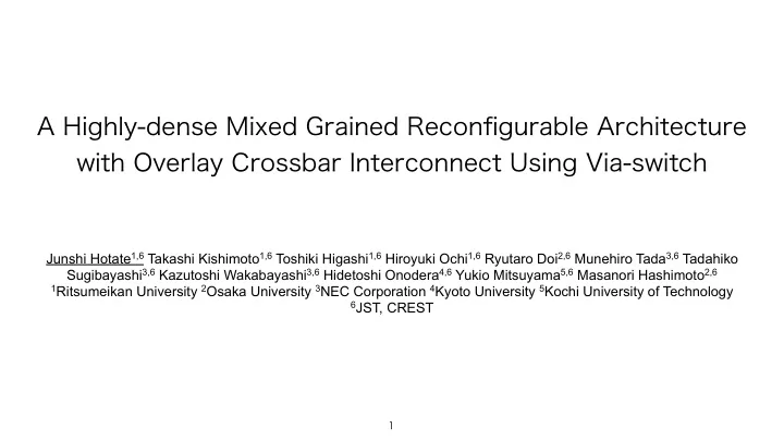
A Highly-dense Mixed Grained Reconfigurable Architecture with Overlay Crossbar Interconnect Using Via-switch 1 Junshi Hotate 1,6 Takashi Kishimoto 1,6 Toshiki Higashi 1,6 Hiroyuki Ochi 1,6 Ryutaro Doi 2,6 Munehiro Tada 3,6 Tadahiko Sugibayashi 3,6
A Highly-dense Mixed Grained Reconfigurable Architecture with Overlay Crossbar Interconnect Using Via-switch 1 Junshi Hotate 1,6 Takashi Kishimoto 1,6 Toshiki Higashi 1,6 Hiroyuki Ochi 1,6 Ryutaro Doi 2,6 Munehiro Tada 3,6 Tadahiko Sugibayashi 3,6 Kazutoshi Wakabayashi 3,6 Hidetoshi Onodera 4,6 Yukio Mitsuyama 5,6 Masanori Hashimoto 2,6 1 Ritsumeikan University 2 Osaka University 3 NEC Corporation 4 Kyoto University 5 Kochi University of Technology 6 JST, CREST
Conventional density Arith/ Mem) T1 T2 Contributions Chip area Crossbar Delay Logic Energy 26X -76% -90% -93% Concepts of Proposed Architecture 2 are replaced by Via-Switch . SRAM-based FPGA (LUT/ array FEOL Logic (LUT/ DSP/ Mem) T1 T2 SRAM + MOS Switch Via-Switch All in layers FEOL layers Proposed Architecture BEOL layers FEOL layers set of logic resources. • MOS switches with SRAM elements • Smaller footprint (200F 2 →18F 2 ) • Occupies BEOL layers only • FEOL layers can be used for rich
T1 ③Low parasitic capacitance Via-Switch T1 and T2 are connected and disconnected. Via-switch is a non-volatile and re-programmable switch. <Features> (6F×3F) (0.14fF) ④Multi-fanout support ②Low resistance(on-R 200Ω) T2 ①Small footprint non-volatile resistive RAM to be programmed non-linear device for selecting an atom switch Complementary atom switch Varistors C1 C2 3
Array structure LB Architecture Overview MB or AB XB XB XB XB LB Unit tile LB LB LB LB LB LB blocks (LBs) and a coarse-grained arithmetic block (AB) or memory block (MB). The unit tile consists of four crossbar blocks (XBs), eight fine-grained logic The proposed architecture is a homogeneous array of unit tiles 4
LUT 33 FEOL layers BEOL AB LB XB 5 Architecture Components Logic Block 34 34 17 Arith 32 16 16 16 Arithmetic Block bidirectional interconnect Each wire segment is a To/From East Via-switch(6F×3F) Crossbar To/From West Mem layers
Target Architecture Required logic resources for “CConv” Mapping Experiments <Target Design> <Design Flow> Routing Placement Netlist Technology mapping RTL CWB C for image sensor including RGB-YUV conversion AB We implemented a design “ CConv” , a front-end circuit 4×4 (16AB+128LB) 76 14 MGRA (proposed) 8×8 (512LB) 512 FGRA Unit tile array size LB 6 ―
Circuit simulation result at 0.5V operation using a circuit model of 91×44 crossbar with the equivalent circuit model of the via-switch Results Distance (# of XBs) This improvement can contribute to filling the gap between FPGA and ASIC. Delay [ns] Distance (# of XBs) Energy [pJ] (2)Delay and Energy 85108μm 2 4×4 5319μm 2 308kF 2 426kF 2 44 MGRA bidir. 352512μm 2 8×8 5508μm 2 441kF 2 87kF 2 Comparison of the array area needed for implementing “CConv” (1)Array Area Architecture Track BEOL FEOL area area 7 Tile area Array size Array area FGRA unidir. 68 − 76% − 90% − 93%
Thank you! Please visit my poster.
Recommend
More recommend
Explore More Topics
Stay informed with curated content and fresh updates.
