Highlydense Mixed Grained Reconfigurable Architecture with Viaswitch - PowerPoint PPT Presentation
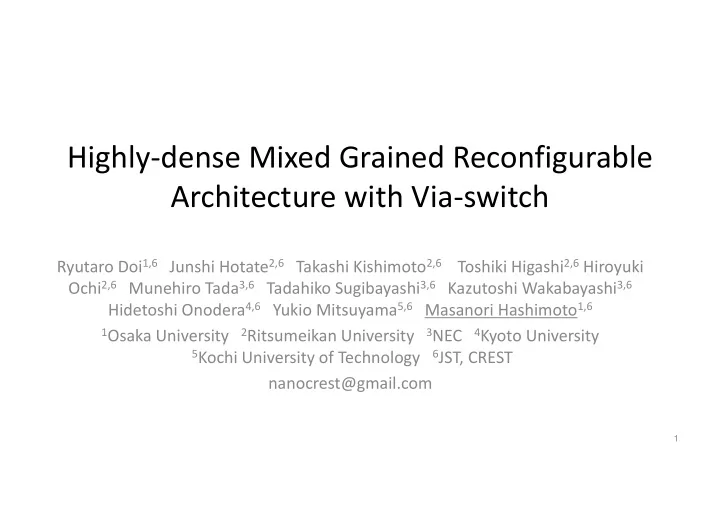
Highlydense Mixed Grained Reconfigurable Architecture with Viaswitch Ryutaro Doi 1,6 Junshi Hotate 2,6 Takashi Kishimoto 2,6 Toshiki Higashi 2,6 Hiroyuki Ochi 2,6 Munehiro Tada 3,6 Tadahiko Sugibayashi 3,6 Kazutoshi Wakabayashi 3,6 Hidetoshi
Highly‐dense Mixed Grained Reconfigurable Architecture with Via‐switch Ryutaro Doi 1,6 Junshi Hotate 2,6 Takashi Kishimoto 2,6 Toshiki Higashi 2,6 Hiroyuki Ochi 2,6 Munehiro Tada 3,6 Tadahiko Sugibayashi 3,6 Kazutoshi Wakabayashi 3,6 Hidetoshi Onodera 4,6 Yukio Mitsuyama 5,6 Masanori Hashimoto 1,6 1 Osaka University 2 Ritsumeikan University 3 NEC 4 Kyoto University 5 Kochi University of Technology 6 JST, CREST nanocrest@gmail.com 1
Contribution 26X higher density 66% smaller interconnect delay at 0.5V “Via-switch” in BEOL SRAM + MOS SW in FEOL C1 C2 Varistor Atom SW T1 T2 T1 T2 BEOL layer FEOL layer Logic Logic (LUT) (Arithmetic/Memory FEOL layer Unit+MUX for LUT) Proposed Architecture Conventional FPGA 2
Via‐switch Program lines C1 Access Tr. unnecessary for programming C2 M8 [Banno, IEDM2015] M7 M6 T1 M5 Signal lines T2 C1 C2 Varistor Atom SW (Complimentary Atom SW) 3 T1 T2 Atom SW : Electrochemical nonvolatile R-change device On-R can be reduced to 200Ω.
Atom SW under intentional programming Atom SW under unintentional programming Why two program lines? On-state Atom SW Off-state Atom SW 1 0 0 With a single 1 2 program line, 1 unintentional programming 1 will happen. 1 0 0 3 4 Other lines 4 floating
Why two program lines? Atom SW under programming On-state atom SW Off-state atom SW 1 1 With two 0 0 program lines, unintentional 1 2 programming will not happen. 1 0 Multiple-ON in a column enables 3 4 multiple fanouts. 1 0 Other lines 5 floating
Proposed crossbar To/From To/From North Long Wire North structure 0 Connection block IN0 IN1 Signals from 4 LUT0 IN2 IN3 Coarse‐ directions can OUT OR grained Bi-directional IN0 be input/outout IN1 block LUT1 → Higher usage IN2 due to multiple IN3 → Smaller crossbar OUT fanouts Repeater On-demand repeater Close-packed via-switch insertion To/From To/From → Higher density West East → Smaller crossbar 18F 2 via-switch To/From C1 C2 East Switch block M8 To/From M7 Long Wire West M6 Long Wire T1 M5 To/From To/From South T2 South Long Wire
Interconnect Performance Evaluation (65nm) 10 1 (a) (b) 8 0.8 Energy [pJ] Delay [ns] Smaller crossbar thanks 120 tracks 29% 6 0.6 33% to bidirectional signaling reduction 120 tracks 4 0.4 reduction reduces delay and energy. 80 tracks 2 0.2 80 tracks 0 0 117x80 or 157x120 crossbars 0 10 20 30 40 50 0 10 20 30 40 50 No repeaters Distance (# of CLBs) Distance (# of CLBs) @1.0V 10 2.5 no repeaters no repeaters per 10CLBs per 10CLBs 8 2 Energy [pJ] Delay/energy can be Delay [ns] per 15CLBs per 15CLBs 6 1.5 per 20CLBs per 20CLBs optimized by flexible 4 1 buffering. 2 0.5 (a) (b) 0 0 117x80 crossbar 0 20 40 60 80 0 20 40 60 80 @1.0V 7 Distance (# of CLBs) Distance (# of CLBs)
Comparison w/ SRAM‐based FPGA (TMG+SRAM crossbar) 26X higher area density 10 10 (a) (b) 1.0V 8 8 Energy [pJ] Delay [ns] Conventional 35% Conventional 6 6 71% reduction 4 4 reduction 2 2 117x80 crossbar Proposed Proposed repeater inserted 0 0 0 20 40 60 80 0 20 40 60 80 Distance (# of CLBs) Distance (# of CLBs) 30 2 (a) (b) 0.5V 25 1.5 Energy [pJ] Delay [ns] Conventional Conventional 20 82% 66% On-R of via-switch 15 1 reduction reduction is independent of 10 0.5 Proposed supply voltage. 5 Proposed 0 0 117x80 crossbar 0 20 40 60 80 0 20 40 60 80 8 repeater inserted Distance (# of CLBs) Distance (# of CLBs)
Conclusion • Proposed a highly‐dense reconfigurable architecture that exploits via‐switch. – 26X higher density – Interconnection delay is reduced by 35% (1.0V) and 66% (0.5V) – Interconnection energy is reduced by 71% (1.0V) and 82% (0.5V) • Future works – Import long wire interconnection – Application mapping and performance evaluation 9
Recommend
More recommend
Explore More Topics
Stay informed with curated content and fresh updates.
