30 nm I n 0.7 Ga 0.3 As I nverted-type HEMT with Reduced Gate - PowerPoint PPT Presentation
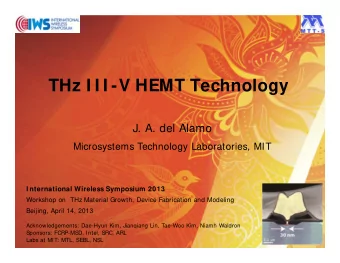
30 nm I n 0.7 Ga 0.3 As I nverted-type HEMT with Reduced Gate Leakage Current g for Logic Applications T.-W. Kim , D.-H. Kim* and J. A. del Alamo Microsystems Technology Laboratories MIT Presently with Teledyne Scientific Sponsors: Intel
30 nm I n 0.7 Ga 0.3 As I nverted-type HEMT with Reduced Gate Leakage Current g for Logic Applications T.-W. Kim , D.-H. Kim* and J. A. del Alamo Microsystems Technology Laboratories MIT Presently with Teledyne Scientific Sponsors: Intel & FCRP-MSD IEDM December 7-9, 2009 Fabrication: MTL, NSL, SEBL Ackno ledgements MBE Technolog for epi Acknowledgements:MBE Technology for epi wafer afer UNIST in Korea for TEM analysis 1
Outline 1. Introduction 2. Device Technology 3. Logic Characteristics 4. Benchmarking with normal HEMT and Si CMOS Si CMOS 5 Conclusions 5. Conclusions 2
I nsulator Scaling in I I I -V HEMTs Motivation : - III-V HEMT: Model system for future III-V logic FETs M ti ti f f - HEMT scaling: L g t ins - Problem: t ins I G -3 10 t ins = 10 nm t ins = 7 nm -4 10 t ins = 4 nm I D -5 10 t ins = 4 nm InAlAs/InGaAs HEMT m] -6 10 L g L g = 30 nm 30 nm I D , I G [A/ I I G <del Alamo, TWHM 09> -7 10 7 nm -8 10 10 nm -9 10 V DS = 0.5 V -10 10 -1.00 -0.75 -0.50 -0.25 0.00 0.25 0.50 V GS [V] • Inverted HEMT design: reduced I G 3
Concept of I nverted HEMT <Normal HEMT > <Normal HEMT > <Inverted HEMT > <Inverted HEMT > Gate Cap. Cap. Insulator Insulator Si Channel Channel doping Barrier Barrier 0.6 3.0 0.6 3.0 Normal HEMT V GS = +0.3 V Inverted HEMT V GS = +0.25 V 2.5 2.5 2.5 0 4 0.4 0.4 0 4 Electron density [ E Electron density 2.0 2.0 Profiles [eV] Profiles [eV] 0.2 0.2 1.5 1.5 0.0 0.0 0 0 0.0 y [x 10 CB P CB P [x 10 1.0 1.0 18 /cm ns,ch = 18 /cm n s,ch = -0.2 -0.2 0.5 0.5 3 ] 1.6 X 10¹²/cm2 1.5 X 10 12 /cm 2 3 ] -0.4 0.0 -0.4 0.0 0 0 10 10 20 20 30 30 40 40 50 50 0 10 20 30 40 50 Vertical depth [nm] Vertical depth [nm] • Lower leakage current due to higher barrier under gate 4
Trade-off of I nverted HEMT : Access region : Contact region 0.8 4 0.8 4 0.6 0.6 Electron Den 3 Electron De 3 0.4 0.4 iles [eV] ile [eV] 0 2 0.2 2 2 0 2 0.2 2 2 ensity [10 nsity [10 CB Profi CB Prof 0.0 0.0 1 1 18 /cm 18 /cm n s,ch = n s,ch = -0.2 -0.2 3 ] 3 ] 0 68 x 10 12 /cm 2 0.6X10 12 /cm 2 0 6X10 12 / 2 0.68 x 10 /cm -0.4 0 -0.4 0 0 10 20 30 40 50 60 70 0 20 40 60 80 100 Vertical depth [nm] Vertical depth [nm] n s,ch ~ 3 x 10 12 /cm 2 for Normal HEMT n s,ch ~ 2.7 x 10 12 /cm 2 for Normal HEMT • Problem: - low n s in access region - large energy barrier under contact region 5
New Approach Gate New doping layer : Access region : Contact region 0.6 4 0.6 4 0.4 0.4 Electron Dens Electron Dens 3 3 ofiles [eV] ofile [eV] 0.2 0.2 2 2 CB Pro sity [10 CB Pro sity [10 0.0 0.0 18 /cm 1 1 18 /cm n s,ch = -0.2 -0.2 n s,ch = 3 ] 2.7X10 12 /cm 2 3 ] 2 4 x 10 12 /cm 2 2.4 x 10 12 /cm 2 2.7X10 /cm -0.4 0 -0.4 0 0 20 40 60 80 0 10 20 30 40 50 60 Vertical depth [nm] Vertical depth [nm] n s,ch ~ 3 x 10 12 /cm 2 for Normal HEMT n s,ch ~ 2.7 x 10 12 /cm 2 for Normal HEMT • High n s in access region • Low barrier in contact region 6
Epitaxial Heterostructure n+ In 0.65 Ga 0.35 As 5 nm Cap n+ In 0.53 Ga 0.47 As 15 nm 0.53 0.47 n+ In 0.52 Al 0.48 As 15 nm Etch stopper InP 6 nm S dop g Si -doping In 0.52 Al 0.48 As 2 nm Barrier In 0.52 Al 0.48 As 8 nm In In 0.53 Ga 0.47 As 2 nm Ga As 2 nm Channel In 0.7 Ga 0.3 As 8 nm In 0.53 Ga 0.47 As 3 nm Back Barrier In 0.52 Al 0.48 As 5 nm n,Hall = 9,800 cm 2 /V-sec + Buffer In 0.52 Al 0.48 As Substrate S. I. InP 7
Device Technology S D Oxide L side L side Cap Cap Etch stopper L g Barrier t ins ins - Triple-recess process t ch Channel - t ins = 4 nm, L side = 80 nm - Gate: Ti/Pt/Au Buffer Buffer - L g : 30 - 130 nm 8
Output & Transfer Char. : L G = 30 nm 0.8 0.6 V DS =0.5 V 1400 0.5 V V GS =0.3 V =0 3 V 1200 1200 0.6 0.4 1000 0.2 G M [mS mA/ m] mA/ m] 800 0.4 0.1 0.3 S/mm] I D [m I D [m 600 0 0.2 400 0.2 -0.1 0.1 200 00 -0.2 0.0 0 0.0 -0.4 -0.2 0.0 0.2 0.4 0.0 0.2 0.4 0.6 0.8 1.0 V GS [V] V DS [V] Good I D saturation, pinch-off behavior G G m = 1.27 S/mm @ V DS =0.5 V 1 27 S/ @ V 0 5 V 9
Subthreshold Char. : L g = 30 nm -3 3 10 I D -4 10 -5 10 V DS = 0.05 V [A/ m] -6 10 V DS = 0.5 V I D & I G [ -7 10 -8 10 I G -9 10 -10 10 -0.6 -0 6 -0 4 -0.4 -0 2 -0.2 0 0 0.0 0.2 0 2 0 4 0.4 V GS [V] • DIBL = 118 mV/V, S = 83 mV/dec. • Excellent I OFF I ON /I OFF = 3.9 X 10 4 for V DS = 0.5 V 10
f T & f max Char. : L g = 30 nm 40 30 U H 21 ] Gain [dB] MAG/MSG 20 f max = 550 GHz 10 V GS =0.2 V f T = 500 GHz V DS 0.8 V V DS =0.8 V 0 9 10 11 12 10 10 10 10 Frequency [Hz] f T =500 GHz & f max =550 GHz Highest f T & f max reported on Inverted HEMTs 11
I nverted vs. Normal HEMTs: I G -3 10 V DS = 0.5 V I D Inverted HEMT Normal HEMT V DS = 50 mV -4 4 DS 10 V DS = 0.5 V L g = 30 nm -5 V DS = 50 mV 10 m] & I G [A/ m -6 6 10 V DS = 50 mV I G -7 10 V DS = 0.5 V I D -8 10 I G -9 10 -10 10 -0.50 -0.25 0.00 0.25 V GS [V] <D -H KIM IPRM 09> <D.-H. KIM IPRM 09> Inverted HEMT: ~100 X less I G than normal HEMT 12
I nverted vs. Normal HEMTs: I ON / I OFF vs. L g -2 7 10 10 Inverted HEMT ION Normal HEMT -3 10 6 6 10 -4 10 -5 A/ m] 10 5 10 I ON & I OFF [A -6 6 I ON /I OFF I 10 4 10 -7 10 -8 10 3 3 10 -9 10 IOFF VDS = 0.5 V -10 2 10 10 20 40 60 80 100 120 140 L g [nm] Inverted HEMT : Excellent I ON /I OFF scalability down to L g = 30 nm 13
I nverted vs. Normal HEMTs: g mi 2 /V-s Inverted HEMT : n,Hall = 9,800 cm 2 /V-s Normal HEMT n,Hall = 11,000 cm 3.2 2.8 g mi from S-parameters g from S parameters m] & g m,ext [S/mm 2.4 2 4 g mi 2.0 g g m,ext t g mi & 1.6 1.2 VDS=0.5V VDS=0 5V 10 100 Gate Length [nm] Inverted HEMTs: Inverted HEMTs: - Lower values of g mi : from reduced and velocity - Better g mi scalability down to 30 nm 14
I nverted vs. Normal HEMTs: R s <Using gate current injection technique> 0.40 Inverted HEMT Inverted HEMT Normal HEMT 0.36 R S =0.27 ohm.mm R sh =100 ohm/sq 0 32 0.32 * [ohm.mm] ] 0.28 R s R 0.24 R sh =70 ohm/sq R S =0.225 ohm.mm R S 0.225 ohm.mm 0.20 0 20 0 40 80 120 160 L g [nm] Higher R s in inverted HEMT Why? Lower n s in access region, higher R c 15
I nverted vs. Normal HEMTs: f T and f max Inverted HEMT 700 0.30 Normal HEMT Inverted HEMT 600 600 Normal HEMT ce g o [S/mm] 0.25 f T 500 f T 0.20 GHz] f max 400 ut conductanc f T & f max [G 0.15 300 f max 0.10 200 Outpu 0.05 100 L g = 30 nm V DS = 0.8 V V DS = 0.8 V L g = 30 nm 0.00 0 -0.3 -0.2 -0.1 0.0 0.1 0.2 0.3 0.4 -0.3 -0.2 -0.1 0.0 0.1 0.2 0.3 0.4 0.5 V V GS [V] [V] V V GS [V] [V] Inverted HEMTs: Lower f & higher f Lower f T & higher f max Improved g o : possibly due to lower n s in access region 16
Benchmarking : SS & DI BL 400 180 Si FETs (IEDM) Si FETs (IEDM) Inverted HEMT pe [mV/dec] ] Inverted HEMT I t d HEMT 160 Normal HEMT Normal HEMT 300 140 V/V] 200 200 hreshold Slo 120 DIBL [mV 100 100 Subth 80 60 0 10 100 10 100 Gate Length [nm] Gate Length [nm] Gate Length [nm] Gate Length [nm] Excellent SCE of inverted HEMT 17 17
Benchmarking : I ON vs. I Leak 1 I ( I I ) -3 x 10 leak OFF G , ON 2 0.5 V DD = 0.5 V InGaAs normal HEMT L g = 30 nm g 65 nm HP-CMOS (L g = 35 nm) 0.4 InGaAs Inverted HEMT L g = 30 nm 0.3 65 nm LP-CMOS (L g = 55nm) N [A/ m] 0 2 0.2 I ON 0.1 0.0 -9 -8 -7 -6 10 10 10 10 I leak [A/ m] At I leak = 100 nA/ μ m, 1.3X higher I ON than 65 nm HP CMOS 18
Benchmarking : CV/ I vs. L g 10 Inverted HEMTs Normal HEMTs AY [psec] 1 1 GATE DELA I In 0.7 Ga 0.3 As HEMTs G A HEMT (V DD = 0.5V) G Si NMOSFETs (V DD = 1.1~1.3V) 0.1 0 1 2 3 10 10 10 10 Gate Length, L g [nm] Inverted HEMT : Comparable Gate delay with L g but at lower V DD < Ref. : Chau et al. (T-Nano 2005) > 19
Conclusions • Inverted InGaAs HEMT – S Scaling benefit: li b fit • Reduced I g allows for further L g scaling – At 30 At 30 nm, inverted HEMTs exhibit excellent characteristics: i t d HEMT hibit ll t h t i ti DIBL < 120 mV/V, S < 85 mV/dec and I ON /I OFF ~ 4 x 10 4 • f > 500 GHz and f f T > 500 GHz and f max > 550 GHz, CV/I ~ 1 psec > 550 GHz CV/I ~ 1 psec • • Inverted InGaAs HEMT: promising layer structure for future Inverted InGaAs HEMT: promising layer structure for future • high-K/III-V MOSFET 20 20
Recommend
More recommend
Explore More Topics
Stay informed with curated content and fresh updates.
