When (Low ) Pow er Really Matters When (Low ) Pow er Really Matters - PowerPoint PPT Presentation
When (Low ) Pow er Really Matters When (Low ) Pow er Really Matters When (Low ) Pow er Really Matters When (Low ) Pow er Really Matters Yogesh K. Ramadass, AnanthaGroup Microsystems Technology Laboratory Outline Outline Outline Outline
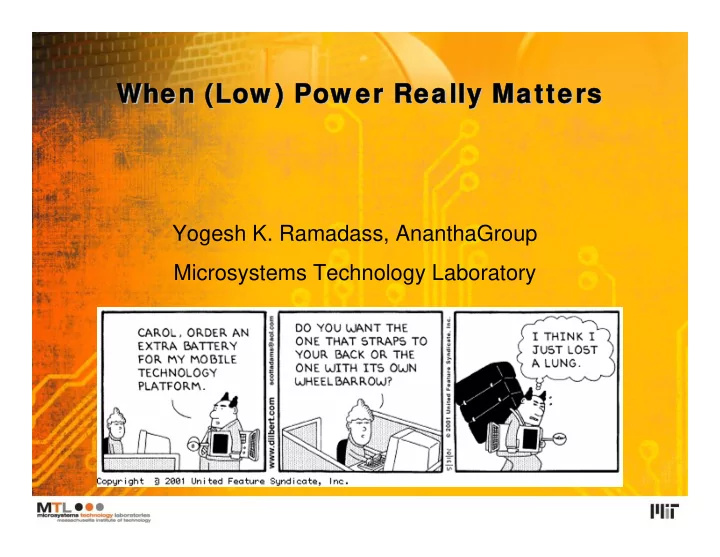
When (Low ) Pow er Really Matters When (Low ) Pow er Really Matters When (Low ) Pow er Really Matters When (Low ) Pow er Really Matters Yogesh K. Ramadass, AnanthaGroup Microsystems Technology Laboratory
Outline Outline Outline Outline � Introduction � Voltage Scaling techniques � Challenges with Low voltage operation � System Examples � Conclusion
Moore Moore ’ ’s Law s Law s Law Moore Moore s Law Gordon Moore Co-founder, INTEL � No. of transistors doubles every two years � Not a physical law, started of as a graphical observation � Exponential increase in circuit complexity
Processor Pow er Levels Processor Pow er Levels Processor Pow er Levels Processor Pow er Levels � More Speed � More Power � More Processing � More Power
So Where is the Pow er Lost? So Where is the Pow er Lost? So Where is the Pow er Lost? So Where is the Pow er Lost? � Analog Circuits – Opamps, ADC/DAC’s, Current/Voltage references � Bias Currents � Switches � Digital Circuits – Processors, Memory � Charging up capacitances � Leakage!! � Imagine burning calories when sitting idle � 30% of total power in big microprocessors � More on this later
A simplistic view of process scaling A simplistic view of process scaling A simplistic view of process scaling A simplistic view of process scaling 250, 180, 130, 90, 65, 45, 32, 22 Process Scaling enables Moore’s Law V BAT = 2 E C V cycle L BAT = 2 . Power C V f L BAT s C L � Reduce C L , reduce power ( ) − � Area reduces too!! 2 V V ∝ f BAT T � Area = Cost s . C V L BAT � Faster switches � More processing � Downside, switches don’t turn off completely
Outline Outline Outline Outline � Introduction � Voltage Scaling techniques � Challenges with Low voltage operation � System Examples � Conclusion
Dynamic Voltage Scaling Dynamic Voltage Scaling Dynamic Voltage Scaling Dynamic Voltage Scaling ( ) − 2 V V ∝ f BAT T s . C V L BAT B. Calhoun B. Calhoun Goal: Operate Circuits at just enough voltage
Implementation of a DVS System Implementation of a DVS System Implementation of a DVS System Implementation of a DVS System Change Voltage with change in workload V. Gutnik V. Gutnik 1996 1996
Pow er Savings by DVS Pow er Savings by DVS Pow er Savings by DVS Pow er Savings by DVS Intel Core Duo Processor Power (Normalized) Courtesy : intel.com � Exponential drop � both voltage and frequency scale � Linear drop � only frequency scales, min. voltage
Energy Constrained Applications Energy Constrained Applications Energy Constrained Applications Energy Constrained Applications Micro-sensor networks Medical devices Target Tracking & Detection Portable Electronics RFID Tags (Courtesy of ARL)
Inductive Link Inductive Link Inductive Link Inductive Link � Try to reduce power consumption to fit in energy budget
Sub- Sub -threshold Operation threshold Operation threshold Operation Sub Sub threshold Operation � Sub-threshold logic operates with V DD < V T � Both on and off current are sub-threshold “leakage” 10 0 Strong Inversion Operation: I D (Normalized) 10 - 2 fast, high-energy 10 - 4 Sub-threshold Operation: Speed ∝ I slower, minimum energy D 10 - 6 10 - 8 0 0.2 0.4 0.6 0.8 1 V DD (Normalized)
Minimum Energy Point (MEP) Minimum Energy Point (MEP) Minimum Energy Point (MEP) Minimum Energy Point (MEP) = + E E E TOTAL ACTIVE LEAKAGE ⎛ − ⎞ V DD ⎜ ⎟ = 2 + = 2 + V nV CV I V T C L e th ⎜ ⎟ DD DD OFF D D eff eff ⎝ ⎠ 4 3.5 E op (Normalized) Active 3 � 65nm simulation Energy 2.5 for 7-tap FIR Total 2 Energy filter showing 1.5 MEP minimum energy Leakage 1 operation Energy 0.5 0 0.2 0.4 0.6 0.8 1 1.2 V DD (V)
Motivation Motivation – – Minimum Energy Tracking Minimum Energy Tracking Minimum Energy Tracking Motivation Motivation Minimum Energy Tracking 5 2-taps E op (Normalized) 4.5 5-taps 10-taps 4 12-taps Workload, V MEP E ACTIVE 3.5 Activity 3 2.5 Temperature, E LEAKAGE V MEP 2 Duration of Increasing Leakage 1.5 Workload 1 0.25 0.3 0.35 0.4 0.45 0.5 V DD (V) � Minimum Energy Point (MEP) varies with workload and temperature � MEP moves when ratio of active to leakage energy changes � Tracking the MEP : 0.5X – 1.5X energy savings
Operation of the Energy Minimizing Loop Operation of the Energy Minimizing Loop Operation of the Energy Minimizing Loop Operation of the Energy Minimizing Loop V DD starts at 420mV V DD starts at 420mV V DD settles at 370mV V DD settles at 370mV Y. Ramadass Y. Ramadass V DD V DD 370mV 370mV 320mV 320mV Loop Stop Loop Stop Loop Start Loop Start
Parallelism Parallelism Parallelism Parallelism � Reduce Voltage � Slower Operation � Parallel banks � Recover Performance � Low power, with good performance (best of both worlds) 400mV 100Mbps baseband processor Demodulation 5 Tap FIR Filter Bit Decoder Correlator Bank Serial to Parallel 5-bit Input from ADC Retiming Block Demodulated 5 Tap FIR Filter FIR Correlator Sub-bank 1 Bits Coefficients 5 Tap FIR Filter Correlator 1 5 Tap FIR Filter Correlator 2 … … … Correlator L Correlator Sub-bank 2 Threshold Detector/ L = 20 Position Encoder Correlator L+1 ……… Correlator L+2 M = 31 … … … Correlator 2L Total # of correlators = 620 … … … V. Sze V. Sze Correlator Sub-bank M Correlator (M-1)L+1 Correlator (M-1)L+2 … … … Acquisition/ Correlator ML Timing Control
Outline Outline Outline Outline � Introduction � Voltage Scaling techniques � Challenges with Low voltage operation � System Examples � Conclusion
A Typical System A Typical System A Typical System A Typical System Extreme Voltage Scaling: Power Supplies Sub-threshold Operation Modeling and Theory V − DD = + 2 2 nV E C V W L KC V e th DMA Total eff DD eff DP g DD Accelerators Standby Power Reduction - Fine-grained power down - Standby voltage scaling Data Memory Instruction Sub-V T Memory DSP Cache Ultra-Dynamic Voltage Scaling Radio Sensor(s)
Challenges w ith sub Challenges w ith sub- -threshold logic threshold logic threshold logic Challenges w ith sub Challenges w ith sub threshold logic Strong 0.4 N1 N2 N3 Q N2 D 0.35 N3, non- 0.3 CK CK ratioed 0.25 Weak N1 0.2 Weak CK Ratioed FF 0.15 Strong N2 N1 N3 0.1 Q D N3 0.05 CK 0 CK 0 20 40 60 80 100 120 Weak time (ns) Weak Ratioed FF fails to write a 1 at Non-ratioed FF strong N, weak P corner at 400mV
Challenges w ith sub Challenges w ith sub- -threshold logic threshold logic threshold logic Challenges w ith sub Challenges w ith sub threshold logic Order of Magnitude Higher Variability in Sub- -V V T Order of Magnitude Higher Variability in Sub T Functionality Performance Global Local J.Kw ong J.Kw ong � Local V T variation → large spread in voltage swing, delay, energy � Errors due to degraded noise margins and timing violations � Variation-tolerant circuits (e.g. asynchronous logic, soft error correction)
A 180mV FFT Processor A 180mV FFT Processor A 180mV FFT Processor A 180mV FFT Processor A. Wang A. Wang � FFT – Fast Fourier Transform � Operates down to 180mV!!! � 5X savings in energy at the minimum energy point
SRAM Challenges SRAM Challenges SRAM Challenges SRAM Challenges Problem 2 Problem #1 Bitline leakage impacts read value: Cannot read correctly!! Feedback too strong: Cannot write new data!! WL WL BLB BL Problem 3 Static Noise Margin (SNM) degraded by variation: Cannot hold data during read!! � Lowest previous demonstrated SRAM in 65nm is 0.7V
Sub Sub- -threshold SRAM design threshold SRAM design threshold SRAM design Sub Sub threshold SRAM design � 8-transistor SRAM cell � Operates down to 350mV!!! � 20X leakage power savings N. Verma N. Verma
Outline Outline Outline Outline � Introduction � Voltage Scaling techniques � Challenges with Low voltage operation � System Examples � Conclusion
Wireless Sensor Netw orks Wireless Sensor Netw orks Wireless Sensor Netw orks Wireless Sensor Netw orks ADC ADC DSP DSP RF RF ADC ADC ADC ADC Se Se Sens Sens nsor nsor or D or D DSP DSP Low -Ra Low -Ra Rate Rate te RF te RF RF RF � Scalable rate � Scalable rate � 16-bit DSP with FFT � 16-bit DSP with FFT � On-Off Keying using a � On-Off Keying using a (0-100KS/s) and (0-100KS/s) and (128-1024 points) (128-1024 points) rectification based rectification based precision (12b & 8b) precision (12b & 8b) receiver receiver � 10pJ/instuction � 10pJ/instuction � 25mW at 100kS/s � 25mW at 100kS/s � Rx Energy: 1-3 nJ/bit � Rx Energy: 1-3 nJ/bit [D. Finchelstein [D. Finchelstein D. Finchelstein D. Finchelstein [N. Verma] [N. Verma] [D. Daly] [D. Daly] and N. Ickes ] and N. Ickes ] and N. Ickes and N. Ickes
Recommend
More recommend
Explore More Topics
Stay informed with curated content and fresh updates.


