VLSID 2016 KOLKATA, INDIA January 4-8, 2016 Massed Refresh: An - PowerPoint PPT Presentation
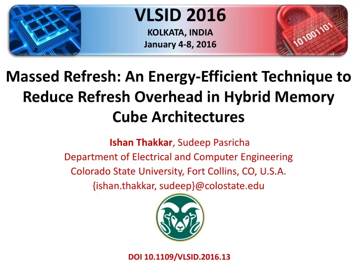
VLSID 2016 KOLKATA, INDIA January 4-8, 2016 Massed Refresh: An Energy-Efficient Technique to Reduce Refresh Overhead in Hybrid Memory Cube Architectures Ishan Thakkar , Sudeep Pasricha Department of Electrical and Computer Engineering
VLSID 2016 KOLKATA, INDIA January 4-8, 2016 Massed Refresh: An Energy-Efficient Technique to Reduce Refresh Overhead in Hybrid Memory Cube Architectures Ishan Thakkar , Sudeep Pasricha Department of Electrical and Computer Engineering Colorado State University, Fort Collins, CO, U.S.A. {ishan.thakkar, sudeep}@colostate.edu DOI 10.1109/VLSID.2016.13
Outline • Introduction • Background on DRAM Structure and Refresh Operation • Related Work • Contributions • Evaluation Setup • Evaluation Results • Conclusion 1
Outline • Introduction • Background on DRAM Structure and Refresh Operation • Related Work • Contributions • Evaluation Setup • Evaluation Results • Conclusion 2
Introduction DRAM : • Main memory is DRAM Dynamic Random Access Memory • It is a critical component of all computing systems: server, desktop, mobile, embedded, sensor Word Line • DRAM stores data in cell capacitor Bit Line • Fully charged cell-capacitor logic ‘1’ Cell • Fully discharged cell-capacitor logic ‘0’ Access Capacitor Transistor • DRAM cell loses data over time, as cell-capacitor leaks charge over time • For temperatures below 85 ° C, DRAM cell loses data in 64ms • For higher temperatures, DRAM cell loses data at faster rate To preserve data integrity, the charge on each DRAM cell (cell-capacitor) must be periodically restored or refreshed . 3
Outline • Introduction • Background on DRAM Structure and Refresh Operation • Related Work • Contributions • Evaluation Setup • Evaluation Results • Conclusion 4
Background on DRAM Structure • Based on their structure, DRAMs are classified in two categories: 1. 2D DRAMs: Planar single layer DRAMs 2. 3D-Stacked DRAMs: Multiple 2D DRAM layers stacked on one-another using TSVs TSV : Through Silicon Via • 2D DRAM structure 2D DRAM Structure Hierarchy Rank Chip Bank Subarray Bitcell 5
2D DRAM: Rank and Chip Structure DRAM Chip DRAM Rank DRAM Chip <N> <N> <N> . . . <N> Mux • 2D DRAM rank: <N> • Multiple chips work in tandem 6
3D-Stacked DRAM Structure In this paper, we consider Hybrid Memory Cube (HMC), which is as a standard for 3D-Stacked DRAMs defined by a consortium of industries HMC Structure Hierarchy Vault Bank Subarray Bitcell Hybrid Memory Cube 7
DRAM Bank Structure 3D-Stacked and 2D DRAMs have similar bank structures Columns Bank Core Bank Subarray Peripherals Row Address Decoder Sense Amplifiers Rows Sense Amplifiers Row Buffer Decoder Column Address Column Mux Data bits 8
DRAM Subarray Structure 3D-Stacked and 2D DRAMs have similar subarray structures Word Line Address Row Bit Line Sense Amps Cell Access Capacitor Transistor Word Line DRAM Bit Line DRAM Cell Cell Sense Amp Sense Amp Sense Amp 9
Basic DRAM Operations PRECHARGE Subarray Dec. EN Global Address =ID? All bitlines of Sense Amplifiers Latch the bank are pre-charged =ID? to 0.5 V DD Subarray Dec. EN Global Row Dec. Sense Amplifiers Row Buffer Column Mux Column Address Decoder 10
Basic DRAM Operations PRECHARGE Subarray ID: 1 ACTIVATION Row 4 Subarray Row 4 Dec. EN Global Address =ID? Sense Amplifiers Latch =ID? The target Row Subarray row is Dec. EN Address opened, Global Row Dec. Sense Amplifiers Row Buffer Column Mux Column Address Decoder 11
Basic DRAM Operations PRECHARGE Subarray ID: 1 ACTIVATION Row 4 Subarray Dec. EN Global Address =ID? Row 4 Sense Amplifiers Latch The target =ID? row is Row Subarray opened, Dec. EN Address then it’s Global captured by Row Dec. Sense Amplifiers SAs Row Buffer Column Mux Column Address Decoder 12
Basic DRAM Operations PRECHARGE Subarray ID: 1 ACTIVATION Row 4 Subarray Row 4 Dec. EN Global Address =ID? Row 4 Sense Amplifiers Latch =ID? SAs drive Row Subarray each bitline Dec. EN Address fully either to Global V DD or 0V – Row Dec. Sense Amplifiers restore the Row Buffer open row Column Mux Column Address Decoder 13
Basic DRAM Operations PRECHARGE Subarray ID: 1 ACTIVATION Row 4 Subarray Row 4 Dec. EN Global Address =ID? Sense Amplifiers Latch =ID? Row Subarray Dec. EN Address Open row is Global stored in Row Dec. Sense Amplifiers global row buffer Row 4 Row Buffer Column Mux Column Address Decoder 14
Basic DRAM Operations PRECHARGE Subarray ID: 1 ACTIVATION Row 4 Subarray READ Row 4 Dec. EN Global Address =ID? Row 4 Sense Amplifiers Latch =ID? Row Subarray Dec. EN Address Target data Global block is Row Dec. Sense Amplifiers selected, Row Buffer and then multiplexed Column Mux out from row Column Column 1 buffer Address Decoder 15
Basic DRAM Operations PRECHARGE Subarray ID: 1 ACTIVATION Row 4 Subarray READ Row 4 Dec. EN Global Address =ID? Row 4 Sense Amplifiers Latch =ID? Row Subarray Dec. EN Address Global Row Dec. Sense Amplifiers Row Buffer A duet of PRECHARGE-ACTIVATION operations restores/refreshes the target row dummy Column Mux Column PRECHARGE-ACTIVATION operations are performed to Column 1 Address refresh the rows Decoder 16
Refresh: 2D Vs 3D-Stacked DRAMs • 3D-Stacked DRAMs have • Higher capacity/density more rows need to be refreshed • Higher power density higher operating temperature (>85 ° C) smaller retention period (time before DRAM cells lose data) of 32ms than that of 64ms for 2D DRAMs • Thus, refresh problem for 3D-Stacked DRAMs is more critical • Therefore, in this study, we target a standardized 3D-Stacked DRAM architecture HMC Refresh Dummy ACTIVATION-PRECHARGE are performed on all rows every retention cycle (32 ms) To prevent long pauses a JEDEC standardized Distributed Refresh method is used 17
Background: Refresh Operation • Distributed Refresh – JEDEC standardized method • A group of 𝑜 rows are refreshed every 3.9 μ s • A group of 𝑜 rows form a ‘ Refresh Bundle (RB)’ • Size of RB increases w/ increase in DRAM capacity increases tRFC Example Distributed Refresh Operation – 1Gb HMC Vault Retention Cycle = 32ms tREFI : Refresh Interval tREFI = 3.9µs tREFI = 3.9µs tREFI = 3.9µs tRFC : tRFC tRFC tRFC Refresh Cycle Time RB1 RB2 RB8192 Size of RB is 16 tRFC tRC : tREC tREC tREC tREC tRC tRC tRC tRC tRC tRC Row Cycle Time Row1 Row2 Row3 Row4 Row15 Row16 tRFC = time taken to refresh entire RB 18
Performance Overhead of Distributed Refresh Source: J Liu+, ISCA 2012 Performance overhead of refresh increases with increase in device capacity 19
Energy Overhead of Distributed Refresh Source: J Liu+, ISCA 2012 Energy overhead of refresh increases with increase in device capacity 20
Energy Overhead of Distributed Refresh Source: J Liu+, ISCA 2012 Refresh is a growing problem, which needs to be addressed to realize low-latency, low-energy DRAMs Energy overhead of refresh increases with increase in device capacity 21
Outline • Introduction • Background on DRAM Structure and Refresh Operation • Related Work • Contributions • Evaluation Setup • Evaluation Results • Conclusion 22
Related Work Scattered Refresh improves upon Per-bank Refresh and All-bank Refresh 23 We improve upon Scattered Refresh
All-Bank Refresh Vs Per-Bank Refresh • Distributed Refresh can be implemented at two different granularities • All-bank Refresh: All banks are refreshed simultaneously, and none of the banks is allowed to serve any request until refresh is complete • Supported by all general purpose DDRx DRAMs • DRAM operation is completely stalled no. of available banks (#AB) is zero • Exploits bank-level parallelism (BLP) for refreshing smaller tRFC • Per-bank Refresh: Only one bank is refreshed at a time, so all other banks are allowed to serve other requests • Supported by LPDDRx DRAMs • #AB > 0 • No BLP larger value of tRFC tRFC : 24 Refresh Cycle Time
All-Bank Refresh Vs Per-Bank Refresh tRFC : • Smaller value of tRFC Refresh Cycle Time All-Bank Refresh • Number of available banks (#AB) = 0 DRAM operation is completely stalled L = Layer ID B = Bank ID SA = Saubarray ID Dummy ACTIVATION-PRECHARGE R = Row ID operations for refresh command Per-Bank Refresh • #AB > 0 tRC : Row Cycle Time • No BLP larger value of tRFC Both All-bank Refresh and Per-bank Refresh have drawbacks and they can be improved 25
Scattered Refresh Source: T Kalyan+, ISCA 2012 • Improves upon Per-bank Refresh – uses subarray-level parallelism (SLP) for refresh • Each row of RB is mapped to a different subarray • SLP gives opportunity to overlap PRECHARGE with next ACTIVATE reduces tRFC Example Scattered Refresh Operation – HMC Vault – Refresh Bundle size of 4 L = Layer ID B = Bank ID SA = Saubarray ID Scattered R = Row ID How does Scattered Refresh compare to Per-bank Refresh and All-bank Refresh ? 26
Scattered Refresh Example Scattered Refresh Operation – HMC Vault – Refresh Bundle size of 4 Per-Bank Scattered tRFC for All-bank Refresh < tRFC for Scattered Refresh < tRFC for Per-bank Refresh All-Bank Room for improvement - Scattered Refresh 27
Outline • Introduction • Background on DRAM Structure and Refresh Operation • Related Work • Contributions • Evaluation Setup • Evaluation Results • Conclusion 28
Recommend
More recommend
Explore More Topics
Stay informed with curated content and fresh updates.


