UMBC A B M A L T F O U M B C I M Y O R T 1 - PowerPoint PPT Presentation
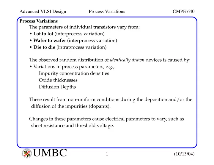
Advanced VLSI Design Process Variations CMPE 640 Process Variations The parameters of individual transistors vary from: Lot to lot (interprocess variation) Wafer to wafer (interprocess variation) Die to die (intraprocess variation)
Advanced VLSI Design Process Variations CMPE 640 Process Variations The parameters of individual transistors vary from: • Lot to lot (interprocess variation) • Wafer to wafer (interprocess variation) • Die to die (intraprocess variation) The observed random distribution of identically drawn devices is caused by: • Variations in process parameters, e.g., Impurity concentration densities Oxide thicknesses Diffusion Depths These result from non-uniform conditions during the deposition and/or the diffusion of the impurities (dopants). Changes in these parameters cause electrical parameters to vary, such as sheet resistance and threshold voltage. L A N R Y D UMBC A B M A L T F O U M B C I M Y O R T 1 (10/13/04) I E S R C E O V U I N N U T Y 1 6 9 6
Advanced VLSI Design Process Variations CMPE 640 Process Variations Causes for observed random distribution (cont): • Variations in the dimensions of the devices: Limited resolution of the photolithographic process which causes W/L variations in MOS transistors. Many design parameters are totally uncorrelated. Variations in MOS transistor length are unrelated to variations in V T . Observations: • Process variations impact the parameters that determine circuit perfor- mance, e.g., transistor current. • V T can vary due to (1) changes in oxide thickness, (2) substract, polysilicon and implant impurity levels and (3) surface charge. Accurate control of V T is very important. In the past, it varied up to 50% while today is is controlled within 25-50 mV. L A N R Y D UMBC A B M A L T F O U M B C I M Y O R T 2 (10/13/04) I E S R C E O V U I N N U T Y 1 6 9 6
Advanced VLSI Design Process Variations CMPE 640 Process Variations • The main cause of variations in process transconductance, k’ n is changes in oxide thickness. • Variations in W and L are caused by the lithographic process. These variations are not correlated because W is determined in the field oxide step while L is defined in the poly and src/drain diffusion steps. These variations results in dramatic changes in device performance charac- teristics, in positive and negative directions. This effects the design process, since your design is constrained by a specifi- cation, e.g., has to run at 3 GHz. In order to account for these variations, you may design your circuit using worst case values for all device parameters. L A N R Y D UMBC A B M A L T F O U M B C I M Y O R T 3 (10/13/04) I E S R C E O V U I N N U T Y 1 6 9 6
Advanced VLSI Design Process Variations CMPE 640 Process Variations While safe, this approach is prohibitively conservative and results in severely over designed and hence uneconomical circuits. Manufacturer usually helps by providing fast and slow as well as nominal device models. An Example: Consider the performance impact of variations on an NMOS transistor in a 0.25 µ m CMOS process. Assume that the device is in saturation with V GS = V DS = 2.5 V. This produces a drain current of 220 µ A. The fast and slow models produce the following values: fast: I D = 265 µ A (+20%) slow: I D = 182 µ A (-17%) Here, W and L are modified by +/- 10%, V T by +/- 60mV and oxide thickness by (+/- 5%). L A N R Y D UMBC A B M A L T F O U M B C I M Y O R T 4 (10/13/04) I E S R C E O V U I N N U T Y 1 6 9 6
Advanced VLSI Design Process Variations CMPE 640 Process Variations Process variations are not the only source of variation that impacts perfor- mance. Variations in the power supply voltage can occur as well. A 10% variations can be expected. fast: V DD = 2.75 V: I D = 302 µ A (+37%) slow: V DD = 2.2.5 V: I D = 155 µ A (-30%) This illustrates that the current levels, and therefore the performance, can vary by as much as 100% over the extremes. In order to guarantee that the fabricated circuits meet performance require- ments, under all circumstances, we need to make the transistor 42% (220 µ A/155 µ A) wider. This results in a severe area penalty. L A N R Y D UMBC A B M A L T F O U M B C I M Y O R T 5 (10/13/04) I E S R C E O V U I N N U T Y 1 6 9 6
Advanced VLSI Design Process Variations CMPE 640 Process Variations Fortunately, it is rare for all parameters to assume their worst (or best-case) values. Most designs will display a performance centered around the nominal design. Design for Manufacturability: Objective is to center the design so that the majority of the fabricated cir- cuit (99%) fall within the performance specifications, while keeping the area overhead minimal. Tools are available to help with this. Monte Carlo analysis involves simulating a circuit over a wide range of randomly chosen device parameters. The result is a distribution plot of design constraints (delay or noise sen- sitivity) that help determine if the nominal design is economically via- ble. L A N R Y D UMBC A B M A L T F O U M B C I M Y O R T 6 (10/13/04) I E S R C E O V U I N N U T Y 1 6 9 6
Advanced VLSI Design Process Variations CMPE 640 Process Variations For example, the impact of effective transistor channel length on the speed of an adder cell. 1.9 Delay (ns) 1.7 1.5 L eff (nm) 1.1 1.5 1.7 1.3 Therefore SPICE simulations should be taken with a grain of salt. The device parameters used in the model are often lot-averaged results. In other words, these parameters are mean values and individual device parameters will vary statistically around these values. L A N R Y D UMBC A B M A L T F O U M B C I M Y O R T 7 (10/13/04) I E S R C E O V U I N N U T Y 1 6 9 6
Advanced VLSI Design Process Variations CMPE 640 Process Variations Modeling inaccuracies and power supply variations are two sources of varia- tion between actual and simulated device performances. Yet a third source of performance variation is temperature . Don’t waste your time tweaking picoseconds out of your design using SPICE. L A N R Y D UMBC A B M A L T F O U M B C I M Y O R T 8 (10/13/04) I E S R C E O V U I N N U T Y 1 6 9 6
Recommend
More recommend
Explore More Topics
Stay informed with curated content and fresh updates.


