UMBC A B M A L F T U M B C I O M Y O T R 1 - PowerPoint PPT Presentation
Principles of VLSI Design Representations CMSC 491B/711 Circuit and System Representations IC design is hard because designers must juggle several different problems: Multiple levels of abstraction: IC designs requires refining an idea
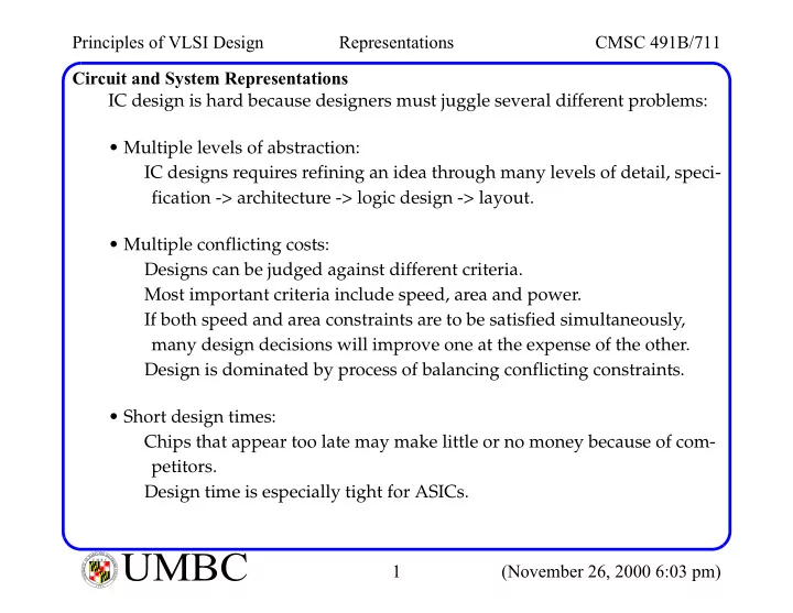
Principles of VLSI Design Representations CMSC 491B/711 Circuit and System Representations IC design is hard because designers must juggle several different problems: • Multiple levels of abstraction: IC designs requires refining an idea through many levels of detail, speci- fication -> architecture -> logic design -> layout. • Multiple conflicting costs: Designs can be judged against different criteria. Most important criteria include speed, area and power. If both speed and area constraints are to be satisfied simultaneously, many design decisions will improve one at the expense of the other. Design is dominated by process of balancing conflicting constraints. • Short design times: Chips that appear too late may make little or no money because of com- petitors. Design time is especially tight for ASICs. L A N R Y D UMBC A B M A L F T U M B C I O M Y O T R 1 (November 26, 2000 6:03 pm) I E S R C E O V U I N N U T Y 1 6 9 6
Principles of VLSI Design Representations CMSC 491B/711 Circuit and System Representations Two techniques used by designers to eliminate unnecessary detail: • Hierarchical design: Divide and conquer, complexity is reduced by recursively breaking it down into manageable parts. Each level of the hierarchy adds complexity by adding components. Commonly used in programming. • Design abstraction: Complexity is reduced by successively replacing detail with simplifica- tions at higher levels of abstraction. Number of components do not change as it is recast to a lower level of abstraction. Less common in programming. Design abstraction and hierarchical design are not the same thing. A design hierarchy uses components at the same level of abstraction. L A N R Y D UMBC A B M A L F T U M B C I O M Y O T R 2 (November 26, 2000 6:03 pm) I E S R C E O V U I N N U T Y 1 6 9 6
Principles of VLSI Design Representations CMSC 491B/711 Circuit and System Representations Performance, interface, cost Specification English area, power requirements Executable Functional Behavioral Simulation Program Design (Behavioral domain) Sequential RTL Simulation; Validation Register Transfer Machines Level Design (Behavioral Domain) Logic Logic Simulation; Verification Logic Design Gates (Structural Domain) Timing Simulation; Circuit Transistors Circuit Design Analysis (Structural Domain) Design Rule Checking Rectangles Layout Design (Physical Domain) L A N R Y D UMBC A B M A L F T U M B C I O M Y O T R 3 (November 26, 2000 6:03 pm) I E S R C E O V U I N N U T Y 1 6 9 6
Principles of VLSI Design Representations CMSC 491B/711 Circuit and System Representations Three design domains: • Behavioral : specifies what a particular system does. • Structural : specifies how entities are connected together. • Physical : specifies how to actually build a structure that has the required connectivity to implement the prescribed behavior. Within each domain, there are many levels of abstraction. L A N R Y D UMBC A B M A L F T U M B C I O M Y O T R 4 (November 26, 2000 6:03 pm) I E S R C E O V U I N N U T Y 1 6 9 6
Principles of VLSI Design Representations CMSC 491B/711 Circuit and System Representations Behavioral: Algorithm written in C, behavioral VHDL or behavioral Verilog, e.g., module triangle (wave); output [0:3]wave; ... always @ ( posedge , clock) begin if (wave == 15) begin inc = -1 end ... Functional simulations would be run to verify the behavior and compliance with the specification. Levels of abstraction include • Algorithmic (HDLs). • Register-level transfer: description of specific hardware registers and the communication between them. • Boolean equations. L A N R Y D UMBC A B M A L F T U M B C I O M Y O T R 5 (November 26, 2000 6:03 pm) I E S R C E O V U I N N U T Y 1 6 9 6
Principles of VLSI Design Representations CMSC 491B/711 Circuit and System Representations Structural: Structural Verilog description module triangle_gen (output, clk, rst); input clk, rst; output [3:0] wave; ... and a1 (s1, output[0], output[1], output[2], output[3]); nor a1 (s2, output[0], output[1], output[2], output[3]); or o1 (s3, s1, s2); ... endmodule; Conversion from behavioral to structural domain may be automatic or man- ual. Simulations would be run to verify compliance with the behavioral specifica- tion. L A N R Y D UMBC A B M A L F T U M B C I O M Y O T R 6 (November 26, 2000 6:03 pm) I E S R C E O V U I N N U T Y 1 6 9 6
Principles of VLSI Design Representations CMSC 491B/711 Circuit and System Representations Structural (cont): Levels of abstraction include • Module level: e.g., cascading of 1-bit adders to form a 4-bit adder. • Gate level: (See above). • Switch level: technology dependent since transistor structure is specified. • Circuit level: SPICE language allows timing behavior to be assessed, e.g., M1 105 107 108 1 pfet L=2.0U W=4.0U R5 102 109 139.0 R6 104 110 195.5 M2 0 109 110 0 nfet L=2.0U W=4.0U R7 104 111 195.5 R8 106 112 139.0 M3 111 112 0 0 nfet L=2.0U W=4.0U C0 104 0 .01P C1 100 0 11F L A N R Y D UMBC A B M A L F T U M B C I O M Y O T R 7 (November 26, 2000 6:03 pm) I E S R C E O V U I N N U T Y 1 6 9 6
Principles of VLSI Design Representations CMSC 491B/711 Circuit and System Representations Physical: Conversion from structural domain to the physical domain may be automatic or manual (e.g. using MAGIC). ‘and’, ‘or’, ‘not’, etc. gates can be mapped to standard cells. Automatic place and route algorithms can be used to construct the layout from the structural description. L A N R Y D UMBC A B M A L F T U M B C I O M Y O T R 8 (November 26, 2000 6:03 pm) I E S R C E O V U I N N U T Y 1 6 9 6
Principles of VLSI Design Representations CMSC 491B/711 Circuit and System Representations Placement involves finding the most suitable arrangement in the 2D plane for the cells in the design. Routing then solves the non-planar interconnection problem created by the placement. From layout, actual transistor sizes and capacitance may be calculated. Simulations may again be run to confirm behavior at required speed and esti- mate power dissipation. Levels of abstraction include • Module level: Rectangle or polygon that specifies outer boundary of all the geometry plus a collection of ports specifying the position, layer and width. • Layout level: transistors, wires and contacts. • Photo-mask information. L A N R Y D UMBC A B M A L F T U M B C I O M Y O T R 9 (November 26, 2000 6:03 pm) I E S R C E O V U I N N U T Y 1 6 9 6
Principles of VLSI Design Representations CMSC 491B/711 Circuit and System Representations Simple behavioral description: x = y + z. Addition is carried out using an n-bit adder, composed of n 1-bit adders. A 1-bit adder has: Input: 2 operands, A and B and a carry input, C. Output: a carry output CO and a sum output S. Boolean equations for a 1-bit adder: S = A.B.C + A.B.C + A.C.B + A.B.C CO = A.B + A.C + B.C L A N R Y D UMBC A B M A L F T U M B C I O M Y O T R 10 (November 26, 2000 6:03 pm) I E S R C E O V U I N N U T Y 1 6 9 6
Principles of VLSI Design Representations CMSC 491B/711 Circuit and System Representations Structural VHDL of CO: ENTITY carry IS PORT(A, B: IN BIT; C: IN BIT; CO: OUT BIT ); END carry; ARCHITECTURE carry_str OF carry IS BEGIN CO <= (A AND B) OR (A AND C) OR (B AND C); END carry; L A N R Y D UMBC A B M A L F T U M B C I O M Y O T R 11 (November 26, 2000 6:03 pm) I E S R C E O V U I N N U T Y 1 6 9 6
Recommend
More recommend
Explore More Topics
Stay informed with curated content and fresh updates.


