UMBC A B M A L T F O U M B C I M Y O R T 1 - PowerPoint PPT Presentation
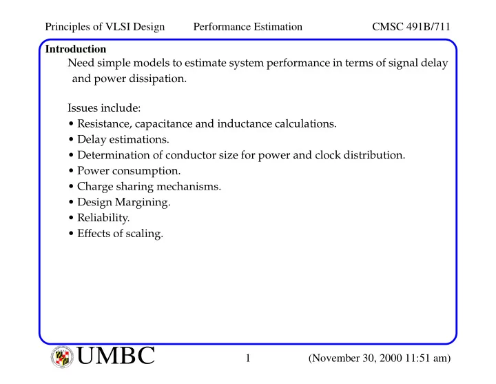
Principles of VLSI Design Performance Estimation CMSC 491B/711 Introduction Need simple models to estimate system performance in terms of signal delay and power dissipation. Issues include: Resistance, capacitance and inductance
Principles of VLSI Design Performance Estimation CMSC 491B/711 Introduction Need simple models to estimate system performance in terms of signal delay and power dissipation. Issues include: • Resistance, capacitance and inductance calculations. • Delay estimations. • Determination of conductor size for power and clock distribution. • Power consumption. • Charge sharing mechanisms. • Design Margining. • Reliability. • Effects of scaling. L A N R Y D UMBC A B M A L T F O U M B C I M Y O R T 1 (November 30, 2000 11:51 am) I E S R C E O V U I N N U T Y 1 6 9 6
Principles of VLSI Design Performance Estimation CMSC 491B/711 Resistance Estimation The resistance of a uniform slab of conducting material may be expressed as ρ - l ρ = resistivity R - Ohms where = - - - - - t w t = thickness l/w = length/width Alternatively as l Ohms R RS R S = sheet resistance in ohms/square. = - - - - where w For example, in a layout editor, such as magic or virtuoso: Typical sheet resistances of 0.5 µ to 1.0 µ processes λ 8 is equivalent to Ω /sq material 16 λ 2 λ Metal1/Metal2 0.07 Metal 3 0.04 Poly 20 4 λ Diffusion 25 n-well Irregular shapes require more elaborate 2K calculation - see text for examples. contacts => 0.25 to 20 ohms. L A N R Y D UMBC A B M A L T F O U M B C I M Y O R T 2 (November 30, 2000 11:51 am) I E S R C E O V U I N N U T Y 1 6 9 6
Principles of VLSI Design Performance Estimation CMSC 491B/711 Resistance Estimation Channel resistance can be estimated in the linear region as: - L Ohms 1 1 Rc - Ohms - - - - - - - - - - - - - - - - - - - - - - - - - - - - - - - - - - - - - - - - - - - - - - - - - - - - - - - - - - - - - - - - - - - - - - - - - - = = µ Cox Vgs ( ) β Vgs ( ) Vt W Vt – – A range of 1,000 to 30,000 ohms/square are possible for n-channel and p- channel devices. Typical betas for identically sized devices; n-dev: ~90, p-dev: ~30 microA/V 2 . Temperature changes both mu (mobility) and V t (threshold voltage) and, therefore channel resistance. Channel resistance increases with temperature, approximately +0.25% per degree C above 25 degrees. Metal and poly resistance change about 0.3% and well diffusions about 1% per degree C. L A N R Y D UMBC A B M A L T F O U M B C I M Y O R T 3 (November 30, 2000 11:51 am) I E S R C E O V U I N N U T Y 1 6 9 6
Principles of VLSI Design Performance Estimation CMSC 491B/711 Capacitance Estimation Switching speed of MOS systems strongly dependent: Parasitic capacitances associated with the MOS transistor. Interconnect capacitance of "wires". Resistance of transistors and wires. Total load capacitance on the output of a CMOS gate is sum of: Gate capacitance (of receiver logic gates downstream). Driver diffusion (source/drain) capacitance. Routing ( line ) capacitance of substrate and other wires. Let’s consider approximations of each of these capacitances and subsequent approximations of delay based on these expressions. Driver C s and C d Receivers C g Line capacitance L A N R Y D UMBC A B M A L T F O U M B C I M Y O R T 4 (November 30, 2000 11:51 am) I E S R C E O V U I N N U T Y 1 6 9 6
Principles of VLSI Design Performance Estimation CMSC 491B/711 Estimating Gate Capacitance: V gs > V t n-MOS transistor - + thickness of Gate thin oxide GND t ox + V ds = 0 Source - Poly Drain C gs C gd C gd GND C gb C db C sb The capacitance of a MOS transistor can be modeled using 5 capacitors. An approximation of gate capacitance (C gs , C gd and C gb ) is given as: Cg CoxA ε SiO 2 ε 0 = Cox = - - - - - - - - - - - - - - - - - - - - - - where C ox is the thin-oxide capacitance per unit area, tox L A N R Y D UMBC A B M A L T F O U M B C I M Y O R T 5 (November 30, 2000 11:51 am) I E S R C E O V U I N N U T Y 1 6 9 6
Principles of VLSI Design Performance Estimation CMSC 491B/711 Estimating Gate Capacitance: For example, for thin-oxide thickness of 15 nm, – 14 × × 10 ⁄ F cm 3.9 8.854 2.3 f F um 2 ⁄ Cox = - - - - - - - - - - - - - - - - - - - - - - - - - - - - - - - - - - - - - - - - - - - - - - - - - - - - - - - - - - - - - = – 7 × 10 cm 15 In λ 4 λ technology, W = 2 and L = 1 = 0.5 2 λ 2 µ m 2 × 2.3 f F µ m 2 ⁄ Cg intrinsic 4.6 fF = = ( ) 2 Typical value for a 1 micron process: 1800 aF µ m ⁄ This is a conservative estimate of gate capacitance that does not include fringing fields (extrinsic) gate capacitance. Gate capacitance increases as the thin-oxide thins. L A N R Y D UMBC A B M A L T F O U M B C I M Y O R T 6 (November 30, 2000 11:51 am) I E S R C E O V U I N N U T Y 1 6 9 6
Principles of VLSI Design Performance Estimation CMSC 491B/711 Estimating Source/Drain Capacitance: An approximation ( lumped model ) of source/drain capacitance (C sb and C db ) is given as: Two components junction periphery Source Gate Drain C sb C db × ( ) × ( ) Cd C ja ab C jp 2 a 2 b = + + where C ja = junction capacitance per µ m 2 C jp = periphery capacitance per µ m a = width of diffusion region ( µ m) b = length of diffusion region ( µ m) This model assumes a zero DC bias across the junction. L A N R Y D UMBC A B M A L T F O U M B C I M Y O R T 7 (November 30, 2000 11:51 am) I E S R C E O V U I N N U T Y 1 6 9 6
Principles of VLSI Design Performance Estimation CMSC 491B/711 Estimating Source/Drain Capacitance: For example: Typical values for 0.5 micron process 4 λ n-device p-device 0.04 f F µ m 2 0.17 f F µ m 2 ⁄ ⁄ C ja 6 λ 0.3 f F µ m ⁄ 0.2 f F µ m ⁄ C jp n-channel device fF µ m 2 × × ⁄ ( × × ) × 0.3 fF µ m ⁄ Cd 3.24 fF = 2 3 0.04 + 2 2 + 2 3 = Because of fan-out, gate capacitance usually dominates the loading. L A N R Y D UMBC A B M A L T F O U M B C I M Y O R T 8 (November 30, 2000 11:51 am) I E S R C E O V U I N N U T Y 1 6 9 6
Principles of VLSI Design Performance Estimation CMSC 491B/711 Estimating Routing Capacitance: Routing capacitance between metal and poly can be approximated using a parallel-plate model. fringing fields parallel plate (internodal and substrate) oxide insulator H Usually specified substrate substrate separately capacitance ε A ε = permittivity of the insulator where Cp = - - p t – t = insulator thickness A = area of the parallel-pate capacitor or Cp CSA = where C S is substrate capacitance per unit area. p – The effect of the fringing fields is to increase the effective area of the plates. L A N R Y D UMBC A B M A L T F O U M B C I M Y O R T 9 (November 30, 2000 11:51 am) I E S R C E O V U I N N U T Y 1 6 9 6
Principles of VLSI Design Performance Estimation CMSC 491B/711 Simple Gate Delay Model Appropriate if the wire delay is MUCH less than the gate delay, e.g., 2 τ g In this case, we model the "electrical node" τ w τ g or « l « - - - - - - - - - simply as a capacitive load. rc This expression derives from the expression for RC delay (we’ll see this later). As an example, assuming gate delay is 200ps, what is the maximum length of a minimal-width metal wire (in 1.0um technology) that we can use without worrying about the RC delay of the wire itself? Assume Metal1 = 0.05 Ohms/square and 30 aF/um 2 . 3 λ λ = 0.5 um – 9 × × 10 2 0.2 16 330 λ , l « - - - - - - - - - - - - - - - - - - - - - - - - - - - - - - - - - - - - - - - - - - - - - - - - - - - = – 18 3 λ × 10 × 0.05 30 3 × - - - - - - - - - - - - - - - - - - - - - - - - - - - - - - - - - - - - - - - - - - - - 3 λ 2 But this assumes there is no gate load capacitance. A conservative estimate is 5000 lambda (~16,330/3). In a 1.0um process, RC delay MUST be considered for any wire > 2.5mm. L A N R Y D UMBC A B M A L T F O U M B C I M Y O R T 10 (November 30, 2000 11:51 am) I E S R C E O V U I N N U T Y 1 6 9 6
Principles of VLSI Design Performance Estimation CMSC 491B/711 Simple Gate Delay Model But for now, let’s consider "electrical nodes" for which we can ignore distrib- uted RC effects. Our model and definitions: 90% V in (t) V out (t) t dr 50% 10% t f Fall/rise time, e.g. t f , computed between 10% and 90% of V DD . Propagation delay, t dr , computed at 50% points on input and output wave- forms. L A N R Y D UMBC A B M A L T F O U M B C I M Y O R T 11 (November 30, 2000 11:51 am) I E S R C E O V U I N N U T Y 1 6 9 6
Recommend
More recommend
Explore More Topics
Stay informed with curated content and fresh updates.


