UMBC A B M A L T F O U M B C I M Y O R T 1 - PowerPoint PPT Presentation
Advanced VLSI Design Quality Metrics of a Digital Design II CMPE 640 Functionality and Robustness Directivity: Requires a gate to be unidirectional , e.g., changes in an output level should not appear at any unchanging input of the same circuit.
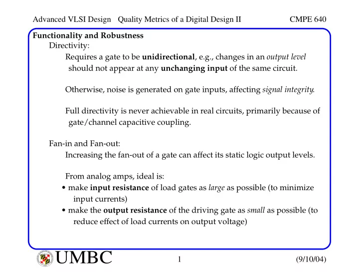
Advanced VLSI Design Quality Metrics of a Digital Design II CMPE 640 Functionality and Robustness Directivity: Requires a gate to be unidirectional , e.g., changes in an output level should not appear at any unchanging input of the same circuit. Otherwise, noise is generated on gate inputs, affecting signal integrity . Full directivity is never achievable in real circuits, primarily because of gate/channel capacitive coupling. Fan-in and Fan-out: Increasing the fan-out of a gate can affect its static logic output levels. From analog amps, ideal is: • make input resistance of load gates as large as possible (to minimize input currents) • make the output resistance of the driving gate as small as possible (to reduce effect of load currents on output voltage) L A N R Y D UMBC A B M A L T F O U M B C I M Y O R T 1 (9/10/04) I E S R C E O V U I N N U T Y 1 6 9 6
Advanced VLSI Design Quality Metrics of a Digital Design II CMPE 640 Functionality and Robustness Fan-in and Fan-out: Large fan-outs also degrade the dynamic performance of the driving gate. Similarly, large fan-ins degrade both static and dynamic properties. The Ideal Digital Gate (from the static perspective): • Has infinite gain in the transition region • Gate threshold is located mid logic swing • High and low noise margins equal to half the swing • Input/output impedances are infinity/zero (unlimited fan-out) V out ∞ g = – V in Impossible but the static CMOS inverter comes close, as we will see. L A N R Y D UMBC A B M A L T F O U M B C I M Y O R T 2 (9/10/04) I E S R C E O V U I N N U T Y 1 6 9 6
Advanced VLSI Design Quality Metrics of a Digital Design II CMPE 640 Performance Expresses the computational load that the circuit can manage. MIPs and FLOPs are used for microprocessors. Here, we focus on performance as it relates to the logic design (as opposed to the architecture). Performance is expressed as clock period or clock frequency . Factors that affect the minimum clock period: • Propagation delay through the logic • Time to get data in and out of the registers • Uncertainty in the clock arrival times (clock skew) At the core of these factors is performance of the individual gate. Let t p represent propagation delay and t pHL and t pLH represent output signal response times. t pHL and t pLH are measured between the 50% points of the input and out- put waveforms. L A N R Y D UMBC A B M A L T F O U M B C I M Y O R T 3 (9/10/04) I E S R C E O V U I N N U T Y 1 6 9 6
Advanced VLSI Design Quality Metrics of a Digital Design II CMPE 640 Performance Define t p as the average of t pHL and t pLH because they are usually not equal: tpLH tpHL + tp = - - - - - - - - - - - - - - - - - - - - - - - - - - - - - - - - - - 2 Note that t p is an artificial gate quality metric (used in broader contexts) while t pHL and t pLH are real measures. V in t V out t pHL t pLH t t f t r L A N R Y D UMBC A B M A L T F O U M B C I M Y O R T 4 (9/10/04) I E S R C E O V U I N N U T Y 1 6 9 6
Advanced VLSI Design Quality Metrics of a Digital Design II CMPE 640 Performance Delay is a function of the slopes of the input and output signals of the gate. The uncertainty in the actual start and stop points is avoided by using the 10% and 90% points. Note that t f and t r are derived from signal waveforms and not the gate. Rise and fall times are affected by: • Strengths of the driving gate • The resistive and capacitive load of the driven node When comparing performance of gates in different technologies or logic styles, load, fan-in and fan-out should not be a factor. v 0 v 1 v 2 v 3 v 4 Ring oscillator L A N R Y D UMBC A B M A L T F O U M B C I M Y O R T 5 (9/10/04) I E S R C E O V U I N N U T Y 1 6 9 6
Advanced VLSI Design Quality Metrics of a Digital Design II CMPE 640 Performance The ring oscillator is the de-facto standard circuit for unbiased delay measure- ments. The period T of the oscillation is: × × T t p N = 2 where N is the # of inverters in the chain. The factor of 2 indicates that a full cycle consists of both a HL and LH transition. This equation holds true only for: 2 Nt p t f t r » + If violated, one wave will overlap with the following, damping the oscil- lation. Note that a value for t p of 20 ps obtained from the ring oscillator does NOT mean that your circuit will operate at 50 GHz! Real designs have fan-ins and fan-outs > 1, and slow-downs of 50 to 100 over the RO frequency are common. L A N R Y D UMBC A B M A L T F O U M B C I M Y O R T 6 (9/10/04) I E S R C E O V U I N N U T Y 1 6 9 6
Advanced VLSI Design Quality Metrics of a Digital Design II CMPE 640 Performance The following first-order RC model is often used to model a digital circuit. R V out Step input produces an exponential transient response. V in C e t τ ⁄ – τ ( ) ( ) V RC v out t where = = 1 – V max value of V in = The time to reach the 50% or 90% point are given as: ( ) τ 0.69 τ t = ln 2 = ( ) τ 2.2 τ t = ln 9 = L A N R Y D UMBC A B M A L T F O U M B C I M Y O R T 7 (9/10/04) I E S R C E O V U I N N U T Y 1 6 9 6
Advanced VLSI Design Quality Metrics of a Digital Design II CMPE 640 Power Consumption Power consumption of a design determines how much energy is consumed per operation and how much heat is dissipated. Affect a number of important design decisions: • Power-supply capacity • Battery lifetime • Supply-line sizing • Packaging • Cooling requirements Different dissipation measures are used depending on the design problem: • Peak power ( P peak ) is important for supply-line sizing. • Average power dissipation ( P av ) is important for cooling and battery life. L A N R Y D UMBC A B M A L T F O U M B C I M Y O R T 8 (9/10/04) I E S R C E O V U I N N U T Y 1 6 9 6
Advanced VLSI Design Quality Metrics of a Digital Design II CMPE 640 Power Consumption Both measures are defined by: [ ( ) ] Ppeak ipeakVsupply max p t = = T T Vsupply 1 ∫ ( ) t ∫ ( ) t Pav p t d isupply t d = - - - = - - - - - - - - - - - - - - - - - - - - - T T 0 0 Where: • p(t) is the instantaneous power. • i supply is the current drawn from the supply voltage V supply over the time interval t in [0.. T ] • i peak is the maximum value of i supply over that interval. Dissipation can be further broken down into: • Static : static conductive paths between the supply rails and leakage cur- rents. • Dynamic : charging capacitors and temporary current paths. It is porportional to the switching frequency. L A N R Y D UMBC A B M A L T F O U M B C I M Y O R T 9 (9/10/04) I E S R C E O V U I N N U T Y 1 6 9 6
Advanced VLSI Design Quality Metrics of a Digital Design II CMPE 640 Power Consumption Propagation delay and power consumption are related. Delay is determined largely by the speed at which a given amount of energy can be stored on gate capacitors. The faster the energy transfer, the higher the power consumption. The faster the energy transfer, the faster the gate. For a given technology and gate topology, the product of power consumption and propagation delay is a constant. Called the Power-Delay Product (PDP). It is the energy consumed by the gate per switching event , and can be used as a quality measure of the switching device. Ideal gate is one that is fast and consumes little energy. The Energy-Delay (E-D) product brings them together and is the ulti- mate measure: E-D = PDP 2 L A N R Y D UMBC A B M A L T F O U M B C I M Y O R T 10 (9/10/04) I E S R C E O V U I N N U T Y 1 6 9 6
Advanced VLSI Design Quality Metrics of a Digital Design II CMPE 640 Power Consumption R V out V in C The total energy delivered by the source is given by: ∞ ∞ V d v out CV 2 ∫ ∫ ∫ ( ) v in t ( ) t - t ( ) E in i in t d V C d CV d v out = = - - - - - - - - - - - - = = dt 0 0 0 Note that the total amount of energy is independent of the resistor R. Energy actually stored on the capacitor : ∞ ∞ V d v out CV 2 ∫ ∫ ∫ ( ) v out t ( ) t E C i C t d C - v out t d C v out v out d = = - - - - - - - - - - - - = = - - - - - - - - - - - dt 2 0 0 0 The other half is dissipated as heat in the resistor. On the falling edge, the energy on the cap is dissipated in the resistor. L A N R Y D UMBC A B M A L T F O U M B C I M Y O R T 11 (9/10/04) I E S R C E O V U I N N U T Y 1 6 9 6
Recommend
More recommend
Explore More Topics
Stay informed with curated content and fresh updates.


