Towards a Reconfigurable Nanocomputer Platform Paul Beckett School - PDF document
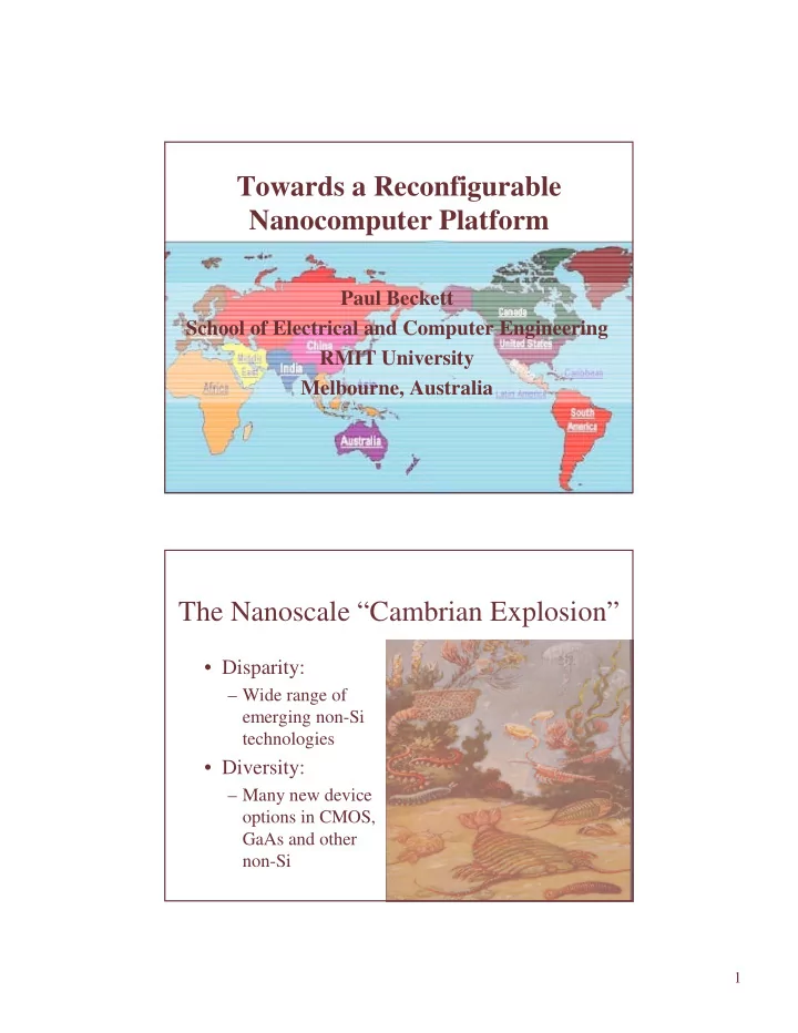
Towards a Reconfigurable Nanocomputer Platform Paul Beckett School of Electrical and Computer Engineering RMIT University Melbourne, Australia 1 The Nanoscale Cambrian Explosion Disparity: Wide range of emerging non-Si
Towards a Reconfigurable Nanocomputer Platform Paul Beckett School of Electrical and Computer Engineering RMIT University Melbourne, Australia 1 The Nanoscale “Cambrian Explosion” • Disparity: – Wide range of emerging non-Si technologies • Diversity: – Many new device options in CMOS, GaAs and other non-Si NSC-1 2 1
Example Nanoscale Devices Disparity → → → → Silicon Hetero- Nanotube Molecular Magnetic Q-Well junction SOI RTD/ CNT Rotaxane GMR/ Quantum dot HFET CMR Si-Ge C60 logic molecular Quantum RTT & memory x-bar MQCA diffraction Dual-gate logic & FET Nanotube CAEN Hybrid- Vertical memory array logic Hall effect Quantum FET Coulomb- Multi- interference Large- coupled Molecular Ballistic valued devices bandgap optically nano- nano-FET logic devices pumped magnetics surface super- nano- (AlN, BN) nanodevices lattices Magnetic pipelining DNA RTD RSFQ 3 The “Ideal” Nanocomputer Platform? • Very large, scalable with rich, local connectivity • Built from simple devices that exhibit: – High functionality (?) – Gain > 1 – Static (at least) and preferably non-volatile operation – (Very) low power density – Room temperature operation • Reliable and fault tolerant • Preferably no intrinsic reliance on any form of global signal (e.g. a master clock) • Reconfigurable in operation, with little or no performance penalty 4 2
Three Example Nanoscale Systems 1. Multi-valued SRAM Based Platform – RTD multi-valued RAM – Dual-gate transistors 2. Phase Transition Device Based Platform – Resistive thin-films 3. A Nano-Magnetic Platform – Double spin-filter junction 5 Multi-valued SRAM Based Platform • metal-insulator tunnel Top Gate gate insulator transistor (MITT) Source Drain – gate voltage modulates the gate insulator Tunnel Back Gate Insulator tunnel barrier substrate • compatible with current 1.0 0.0V fabrication processes V DD A 0.8 – can be buried in oxide layer R L -0.1V 0.6 B • Proposed dual-gate 0.4 -0.2V V G1 V G2 0.2 increases functionality -0.3V C 0 -0.4V – Low-overhead reconfiguration -0.6 -0.4 -0.2 0.0 0.2 6 Second-Gate Voltage 3
Multi-valued SRAM Based Platform • 3-state memory (Wei & Lin) Word Line • V 1-3 matched by adjusting I D V DD3 I P RTD barrier layer thicknesses I V Bit Line V D it Line RTDs RTDs V SS V 1 V 2 V 3 V DD3 V SS Word V DD V SS V SS V DD Line • Ultimate dimensions Substrate 2 insulator 50nm R L R L Out 1 R L • ~3 x 10 9 cells/cm 2 Substrate 1 Gnd 7 Non-volatility – Chalcogenide Films Word Line V A • Chalcogenide films act as fast non-volatile programmable Bit Line resistor V SS word line Polycrystalline TiW • Compatible with current Chalcogenide V dd plane (CMOS) logic fabrication internal routing top gate/input SiO 2 gate insulator Heater • Scales well to nanoscale tunnel insulator gate insulator back gate dimensions (20-30nm) ground plane Al schottky metal • Vertical integration bit line n+ n substrate layer p 8 <100nm 4
Double Spin-Filter Tunnel Junction • Magnetoresistive tunnel device (Worledge & Geballe) – Potentially very high GMR – Formed from two different layers that are insulating but magnetic with unequal coercivities parallel pinned free J nonmagnetic magnetic magnetic nonmagnetic E f electrode barrier barrier electrode pinned free barrier barrier Antiparallel J d d 9 E f Vertical Double Spin-Filter Junction • Resistance is varied free layer inner conductor between the inner pillar and the multiple outer conductors outer conductors (x 4) • Requires ~20 Ǻ films on Substrate “pinned” layer a) Top View b) Side View vertical pillar – No obvious candidates c) Square Mesh • Thickness control and Connections lattice matching will be important 10 5
Spin-Filter Based Platform • RTD substrate adds V DD non-linearity to effect logic • VTT for isolation Vertical FET tunnel junction wordline gate • Junction densities in dielectric BL BL BL vertical excess of 2 x 10 11 /cm 2 channel possible RTD RTD RTD Conductivesubstrate 11 Spatial Computing • Memory Hierarchy memory layers – Tries to hide the cost of moving code and data items from one place to another in Inter-level Dielectric a processor system • 3D memory (Zhang) – Proposed as means memory and processing physically IC substrate closer together 3D ROM Zhang, 2000 12 6
A 3D Reconfigurable Computing Platform • Merged processor/ memory into 3D structure memory/processor layers • Reduced memory performance gap • Extreme memory vertical interconnect bandwidth • Processing-in-memory; base substrate processing-is-memory 3D Processor/memory 13 Reconfigurable Nanoelectronic Devices? PRO CON • Maximizes utility of • Can they be built? small devices • Is the added complexity • Reconfiguration over- justified vs. (say) heads kept small molecular approach? • (Mostly) evolving from • Will they efficiently existing techniques support high-performance computer architectures • Compatible with logic synthesis systems 14 7
What’s Next? • Simulation of nano-magnetic materials • Characterization of typical junctions – e.g. tunneling conductance • Simulation of GMR-based array platform • Development of Spatial Computing techniques suited to this platform 15 And in the long term? • “Decimation followed by diversification” (Gould) • Test against the “environment” – ease of fabrication, cost, ease of use etc. • Extinction for some, consolidation and growth for others 16 8
Towards a Reconfigurable Towards a Reconfigurable Nanocomputer Platform Nanocomputer Platform Thank You Thank You Paul Beckett Paul Beckett 17 9
Recommend
More recommend
Explore More Topics
Stay informed with curated content and fresh updates.
