TIMING CLOSURE TIMING CLOSURE FOR FOR ULTRA DEEP SUBMICRON ULTRA - PowerPoint PPT Presentation
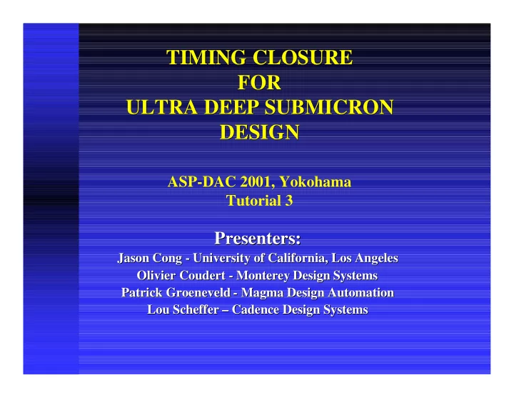
TIMING CLOSURE TIMING CLOSURE FOR FOR ULTRA DEEP SUBMICRON ULTRA DEEP SUBMICRON DESIGN DESIGN ASP-DAC 2001, Yokohama Tutorial 3 Presenters: Presenters: Jason Cong - - University of California, Los Angeles University of California, Los
TIMING CLOSURE TIMING CLOSURE FOR FOR ULTRA DEEP SUBMICRON ULTRA DEEP SUBMICRON DESIGN DESIGN ASP-DAC 2001, Yokohama Tutorial 3 Presenters: Presenters: Jason Cong - - University of California, Los Angeles University of California, Los Angeles Jason Cong Olivier Coudert Coudert - - Monterey Design Systems Monterey Design Systems Olivier Patrick Groeneveld Groeneveld - - Magma Design Automation Magma Design Automation Patrick Lou Scheffer Scheffer – – Cadence Design Systems Cadence Design Systems Lou
Tutorial Outline I Part I: Introduction (Jason Cong) Part I: Introduction (Jason Cong) I I Part II: Timing closure today (Lou Part II: Timing closure today (Lou Scheffer Scheffer) ) I I Part III: Gain Part III: Gain- -based synthesis (Patrick based synthesis (Patrick I Groeneveld) ) Groeneveld I Part IV: Physical design closure (Olivier Part IV: Physical design closure (Olivier I Coudert) ) Coudert I Part V: New approaches to harness global Part V: New approaches to harness global I interconnects (Jason Cong) interconnects (Jason Cong) ASP-DAC'01 Tutorial 3 Timing closure for UDSM design I-2
Tutorial Schedule 09:30am: Introduction (Jason Cong) 09:30am: Introduction (Jason Cong) I 09:40am: Timing closure today (Lou Scheffer Scheffer) ) 09:40am: Timing closure today (Lou I 10:50am Break 10:50am Break I 11:10am: Gain- -based synthesis (Patrick based synthesis (Patrick Groeneveld Groeneveld) ) 11:10am: Gain I 12:30pm: Lunch 12:30pm: Lunch I 02:00pm: The Quest for design closure (Olivier Coudert 02:00pm: The Quest for design closure (Olivier Coudert) ) I 03:20pm: Coffee Break 03:20pm: Coffee Break I 03:40pm: New approaches to harness global interconnects (Jason 03:40pm: New approaches to harness global interconnects (Jason I Cong) Cong) 05:00pm: Wrap- -up and conclusions up and conclusions 05:00pm: Wrap I ASP-DAC'01 Tutorial 3 Timing closure for UDSM design I-3
Exponential Growth of Chip Capacity Moore’s Law Law Moore’s I N Min. transistor feature size decreases by 0.7X every three years Min. transistor feature size decreases by 0.7X every three years N True for at least 30 years! (first published in April 1965) True for at least 30 years! (first published in April 1965) 1997 National Technology Roadmap for Semiconductors 1997 National Technology Roadmap for Semiconductors I Technology (um) 0.25 0.18 0.15 0.13 0.10 0.07 Year 1997 1999 2001 2003 2006 2009 # transistors 11M 21M 40M 76M 200M 520M On-Chip Clock (MHz) 750 1200 1400 1600 2000 2500 Area (mm 2 ) 300 340 385 430 520 620 Wiring Levels 6 6-7 7 7 7-8 8-9 I Enables system Enables system- -on on- -a a- -chip integration chip integration I ASP-DAC'01 Tutorial 3 Timing closure for UDSM design I-4
Productivity Gap - Where Moore Law May Break Logic Transistors/Chip (K) Transistor/Staff-Month 10,000,000 100,000,000 1,000,000 10,000,000 58%/Yr. Complexity 100,000 1,000,000 growth rate 10,000 100,000 1,000 10,000 21%/Yr. x x 100 1,000 x x Productivity growth rate x x x x 10 100 1 10 1998 2003 Chip Capacity and Designer Productivity Source: NTRS’97 ASP-DAC'01 Tutorial 3 Timing closure for UDSM design I-5
Approaches to Increase Design Productivity I Raise level of design abstraction Raise level of design abstraction I I Use hierarchical design Use hierarchical design I Both require synthesis and layout timing closure Both require synthesis and layout timing closure ASP-DAC'01 Tutorial 3 Timing closure for UDSM design I-6
Levels of Abstraction in VLSI Design Behavior-level Synthesis Hardware Description Language Logic-level Synthesis Boolean Equations/Networks Physical-level Design Billions of Rectangles ASP-DAC'01 Tutorial 3 Timing closure for UDSM design I-7
Difficulties in Maintaining High-Level Abstraction & Hierarchical Design I Interconnect delay far dominates device delay Interconnect delay far dominates device delay I N Can no longer design in behavior/functional domain Can no longer design in behavior/functional domain N Technology (um) 0.25 0.18 0.15 0.13 0.10 0.07 Intrinsic gate delay (ns) 0.071 0.051 0.049 0.045 0.039 0.022 1mm (ns) 0.059 0.049 0.051 0.044 0.052 0.042 2cm no-opt (ns) 2.589 2.48 2.65 2.62 3.73 4.67 2cm best-opt (ns) 0.895 0.793 0.77 0.7 0.77 0.672 • Best-opt uses simultaneous buffer insertion, driver/buffer sizing, and wiresizing • Reverse scaling of higher metal layers were not considered • Source: [Cong97] SRC Working Papers http://www.src.org/research/frontier.dgw ASP-DAC'01 Tutorial 3 Timing closure for UDSM design I-8
Difficulties in Maintaining High-Level Abstraction & Hierarchical Design I Current design hierarchy is based on Current design hierarchy is based on I functionality functionality N interconnect delay interconnect delay N N crosstalk crosstalk N N P/G bounce due to simultaneous switching, etc … P/G bounce due to simultaneous switching, etc … N => do not fit naturally into function hierarchy => do not fit naturally into function hierarchy ASP-DAC'01 Tutorial 3 Timing closure for UDSM design I-9
Coupling Noise Problem 0.350 0.300 a pair of in-phase aggressors 0.250 a pair of skewed Noise / Vdd 0.200 0.150 one aggressor 0.100 0.050 0.000 250 180 150 100 70 Technology (nm) Coupling noise from two adjacent aggressors to the middle victim wire (1 mm) with 2x min. spacing. Rise time is 10% of projected clock period. • Coupling noise depends strongly on both spatial and temporal relations! ASP-DAC'01 Tutorial 3 Timing closure for UDSM design I-10
Tutorial Outline I Part I: Introduction (Jason Cong) Part I: Introduction (Jason Cong) I I Part II: Timing closure today (Lou Part II: Timing closure today (Lou Scheffer Scheffer) ) I I Part III: Gain Part III: Gain- -based synthesis (Patrick based synthesis (Patrick I Groeneveld) ) Groeneveld I Part IV: Physical design closure (Olivier Part IV: Physical design closure (Olivier I Coudert) ) Coudert I Part V: New approaches to harness global Part V: New approaches to harness global I interconnects (Jason Cong) interconnects (Jason Cong) ASP-DAC'01 Tutorial 3 Timing closure for UDSM design I-11
Recommend
More recommend
Explore More Topics
Stay informed with curated content and fresh updates.
