Systems Logic Gates and Electrical Properties Shankar Balachandran* - PowerPoint PPT Presentation
Spring 2015 Week 5 Module 23 Digital Circuits and Systems Logic Gates and Electrical Properties Shankar Balachandran* Associate Professor, CSE Department Indian Institute of Technology Madras *Currently a Visiting Professor at IIT Bombay
Spring 2015 Week 5 Module 23 Digital Circuits and Systems Logic Gates and Electrical Properties Shankar Balachandran* Associate Professor, CSE Department Indian Institute of Technology Madras *Currently a Visiting Professor at IIT Bombay
CMOS Transistors Logic Gates and Electrical Properties 2
NMOS and PMOS Logic Gates and Electrical Properties 3
CMOS Inverter V dd (“ 1 ”) 1 out out in in 0 0 1 GND (“ 0 ”) Logic Gates and Electrical Properties 4
CMOS NAND and NOR Gates Logic Gates and Electrical Properties 5
CMOS Inverter Transfer Characteristics P on V out N off V dd 2.5 2 Output 1.5 1 0.6 P off N on V in 0.6 2 0 1 1.5 2.5 V inv V dd Input Logic Gates and Electrical Properties 6
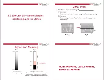
Logic Levels: I/O Voltages V out slope = -1 “1” V OH V OH V IH Undefined Region V IL “0” V OL slope = -1 V OL V in V IL V IH Nominal Voltage Levels: V IH = min. input voltage for logic 1 V IL = max. input voltage for logic 0 V OH = min. output voltage for logic 1 V OL = max. output voltage for logic 0 Logic Gates and Electrical Properties 8
DC Noise Margins High State DC Noise Margin: “1” V OH NM H = V OH - V IH NM H V IH Undefined Region V IL NM L Low State DC Noise Margin: “0” V OL NM L = V IL - V OL Noise margin is a meaningful means for measuring the robustness of a circuit against noise. Logic Gates and Electrical Properties 9
Noise Margins in a CMOS Inverter Logic Gates and Electrical Properties 10
Other Properties Current: Very little current flows in the gate except while it is switching.This is why CMOS is used in low power applications such as digital clocks. Static Power: Steady state or static power consumption is negligible and is due to leakage currents. However, for sub-100nm ( ultra-deep submicron ) CMOS technologies this power is becoming comparable to other power components. Logic Gates and Electrical Properties 11
Capacitances Logic Gates and Electrical Properties 12
Resistance Treat transistor as a resistor In reality, there are several resistances Also, resistance values are different in different modes of operation of a transistor 13 Logic Gates and Electrical Properties
Other Properties (contd…) Dynamic Power: A CMOS circuit consumes significant power only during the switching.This is called dynamic power , P D . Dynamic power consumption depends on the total load capacitance, C L , which is to be charged and discharged at the gate output, and the switching frequency. D 2 P C V f L DD where, C L = C load + gate output capacitance + C wire f = output switching frequency Short Circuit Power: This is the other component of power dissipation which occurs during switching. It is due to the flow of short circuit (or through ) current between V dd and GND. Logic Gates and Electrical Properties 14
Other Electrical Properties Fanout: The number of inputs that are driven by a single output is known as the fanout of the output. A practical limit on fanout is caused by load (capacitance, C L ) on the gate output which must charge/discharge when signal levels change. Fanin: The number of inputs that a gate can have is called the fanin . Higher fanin usually means higher delay (because of transistors in series) Logic Gates and Electrical Properties 15
End of Week 5: Module 23 Thank You Logic Gates and Electrical Properties 16
Recommend
More recommend
Explore More Topics
Stay informed with curated content and fresh updates.

