Standard Cell Library/Library Exchange Format (LEF) Advanced VLSI - PowerPoint PPT Presentation
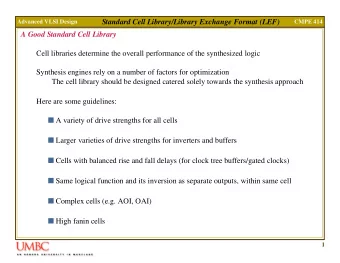
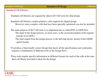
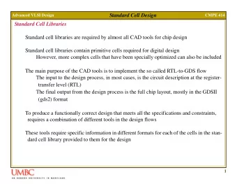
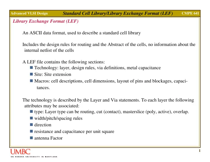
Standard Cell Library/Library Exchange Format (LEF) Advanced VLSI Design CMPE 641 Library Exchange Format (LEF) An ASCII data format, used to describe a standard cell library Includes the design rules for routing and the Abstract of the cells,
Standard Cell Library/Library Exchange Format (LEF) Advanced VLSI Design CMPE 641 Library Exchange Format (LEF) An ASCII data format, used to describe a standard cell library Includes the design rules for routing and the Abstract of the cells, no information about the internal netlist of the cells A LEF file contains the following sections: � Technology: layer, design rules, via definitions, metal capacitance � Site: Site extension � Macros: cell descriptions, cell dimensions, layout of pins and blockages, capaci- tances. The technology is described by the Layer and Via statements. To each layer the following attributes may be associated: � type: Layer type can be routing, cut (contact), masterslice (poly, active), overlap. � width/pitch/spacing rules � direction � resistance and capacitance per unit square � antenna Factor 1
Standard Cell Library/Library Exchange Format (LEF) Advanced VLSI Design CMPE 641 Library Exchange Format (LEF) Layers are defined in process order from bottom to top poly masterslice cc cut metal1 routing via cut metal2 routing via2 cut metal3 routing Cut Layer definition LAYER layername TYPE CUT; SPACING Specifies the minimum spacing allowed between via cuts on the same net or different nets. This value can be overridden by the SAMENET SPACING statement (we are going to use this statement later) END layerName 2
Standard Cell Library/Library Exchange Format (LEF) Advanced VLSI Design CMPE 641 Library Exchange Format (LEF) Implant Layer definition LAYER layerName TYPE IMPLANT ; SPACING minSpacing END layerName Defines implant layers in the design. Each layer is defined by assigning it a name and simple spacing and width rules. These spacing and width rules only affect the legal cell placements. These rules interact with the library methodology, detailed placement, and filler cell support. Masterslice or Overlap Layer definition LAYER layerName TYPE {MASTERSLICE | OVERLAP} ; Defines masterslice (nonrouting) or overlap layers in the design. Masterslice layers are typically polysilicon layers and are only needed if the cell MACROs have pins on the polysilicon layer. 3
Standard Cell Library/Library Exchange Format (LEF) Advanced VLSI Design CMPE 641 Library Exchange Format (LEF) Routing Layer definition LAYER layerName TYPE ROUTING ; DIRECTION {HORIZONTAL | VERTICAL} ; PITCH distance ; WIDTH defWidth ; OFFSET distance ; SPACING minSpacing; RESISTANCE RPERSQ value ; Specifies the resistance for a square of wire, in ohms per square. The resistance of a wire can be defined as RPERSQU x wire length/wire width CAPACITANCE CPERSQDIST value ; Specifies the capacitance for each square unit, in picofarads per square micron. This is used to model wire-to-ground capacitance. 4
Standard Cell Library/Library Exchange Format (LEF) Advanced VLSI Design CMPE 641 Library Exchange Format (LEF) Manufacturing Grid MANUFACTURINGGRID value ; Defines the manufacturing grid for the design. The manufacturing grid is used for geometry alignment. When specified, shapes and cells are placed in locations that snap to the manufacturing grid. Via VIA viaName DEFAULT TOPOFSTACKONLY FOREIGN foreignCellName [ pt [ orient ]] ; RESISTANCE value ; {LAYER layerName ; {RECT pt pt ;} ...} ... END viaName Defines vias for usage by signal routers. Default vias have exactly three layers used: a cut layer, and two layers that touch the cut layer (routing or masterslice). The cut layer rectangle must be between the two routing or masterslice layer rectangles. 5
Standard Cell Library/Library Exchange Format (LEF) Advanced VLSI Design CMPE 641 Library Exchange Format (LEF) Via Rule Generate VIARULE viaRuleName GENERATE LAYER routingLayerName ; { DIRECTION {HORIZONTAL | VERTICAL} ; OVERHANG overhang ; METALOVERHANG metalOverhang ; | ENCLOSURE overhang1 overhang2 ;} LAYER routingLayerName ; { DIRECTION {HORIZONTAL | VERTICAL} ; OVERHANG overhang ; METALOVERHANG metalOverhang ; | ENCLOSURE overhang1 overhang2 ;} LAYER cutLayerName ; RECT pt pt ; SPACING xSpacing BY ySpacing ; RESISTANCE resistancePerCut ; END viaRuleName Defines formulas for generating via arrays. Use the VIARULE GENERATE statement to cover special wiring that is not explicitly defined in the VIARULE statement. 6
Standard Cell Library/Library Exchange Format (LEF) Advanced VLSI Design CMPE 641 Library Exchange Format (LEF) Same-Net Spacing SPACING SAMENET layerName layerName minSpace [STACK] ; ... END SPACING Defines the same-net spacing rules. Same-net spacing rules determine minimum spacing between geometries in the same net and are only required if same-net spacing is smaller than different-net spacing, or if vias on different layers have special stacking rules. Thesespecifications are used for design rule checking by the routing and verification tools. Spacing is the edge-to-edge separation, both orthogonal and diagonal. Site SITE siteName CLASS {PAD | CORE} ; [SYMMETRY {X | Y | R90} ... ;] (will discuss this later in macro definition) SIZE width BY height ; END siteName 7
Standard Cell Library/Library Exchange Format (LEF) Advanced VLSI Design CMPE 641 Library Exchange Format (LEF) Macro MACRO macroName [CLASS { COVER [BUMP] | RING | BLOCK [BLACKBOX] | PAD [INPUT | OUTPUT |INOUT | POWER | SPACER | AREAIO] | CORE [FEEDTHRU | TIEHIGH | TIELOW | SPACER | ANTENNACELL] | ENDCAP {PRE | POST | TOPLEFT | TOPRIGHT | BOTTOMLEFT | BOTTOMRIGHT} } ;] [SOURCE {USER | BLOCK} ;] [FOREIGN foreignCellName [ pt [ orient ]] ;] ... [ORIGIN pt ;] [SIZE width BY height ;] [SYMMETRY {X | Y | R90} ... ;] [SITE siteName ;] [PIN statement ] ... [OBS statement ] ... 8
Standard Cell Library/Library Exchange Format (LEF) Advanced VLSI Design CMPE 641 Library Exchange Format (LEF) Defining Symmetry 9
Standard Cell Library/Library Exchange Format (LEF) Advanced VLSI Design CMPE 641 Library Exchange Format (LEF) Macro Pin Statement PIN pinName FOREIGN foreignPinName [STRUCTURE [ pt [ orient ] ] ] ; [DIRECTION {INPUT | OUTPUT [TRISTATE] | INOUT | FEEDTHRU} ;] [USE { SIGNAL | ANALOG | POWER | GROUND | CLOCK } ;] [SHAPE {ABUTMENT | RING | FEEDTHRU} ;] [MUSTJOIN pinName ;] {PORT [CLASS {NONE | CORE} ;] {layerGeometries} ... END} ... END pinName] Macro Obstruction Statement OBS { LAYER layerName [SPACING minSpacing | DESIGNRULEWIDTH value ] ; RECT pt pt ; POLYGON pt pt pt pt ... ; END 10
Recommend
More recommend
Explore More Topics
Stay informed with curated content and fresh updates.
