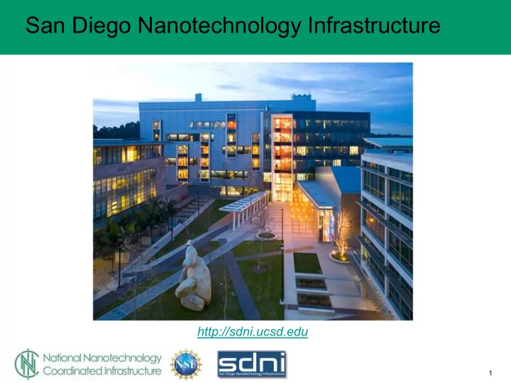

San Diego Nanotechnology Infrastructure http://sdni.ucsd.edu Your Site Logo Here 1
San Diego Nanotechnology Infrastructure 1. SDNI is focused on the areas of NanoBioMedicine, NanoPhotonics , and NanoMagnetism . 2. Support and enable development of cutting edge technology and proof of concept. 3. Accelerate the translation of discoveries and new nanotechnologies to the marketplace , thus increasing economic growths, competitiveness, and high-quality jobs for the nation. Your Site Logo Here 2
San Diego Nanotechnology Infrastructure • Appointed Prof. Oscar Vazquez Mena (Nanoengineering Dept.) as the faculty director for outreach and education. • Appointed Dr. Yves Theriault as the O/E director to spearhead the outreach and education efforts. • Prof. Boubacar Kante joined UC Berkeley. • Mr. Ryan Anderson left SDNI to become cleanroom director for UC Davis. Your Site Logo Here 3
Facilities and Tools Invested >$4M institutional funds into new equipment/upgrades. Received donation of >$1M in equipment. – Added new CMRR Materials Characterization Facility: State-of-the-art tools for thin-film and powder characterization of crystal structure, magnetic, surface, transport and optical properties (XRD, XPS, Hall effect, UV-Vis, AFM/MFM, SEM, etc.). – Purchased 200kV Transmission Electron Microscope (Talos F200X G2 Transmission Electron Microscope with Super-X EDS Detector, Enfinium ER/977 200 kV EELS, Tomography Data Acquisition Software for TEM, STEM, EDS); received internal UCSD funds of ~$3.5M to enable this purchase/installation. – ~$500k additional investments in minor new tools/upgrades. Your Site Logo Here 4
Fueling Scientific Breakthrough Quantum Material Based Spiking Neuristor: Supporting the Big Idea of Convergent Research Demonstrate energy-efficient quantum-materials based devices “Neuristors” which emulate spiking neurons. This allows the use of the internal degrees of freedom of strongly correlated quantum materials to emulate the complex behavior of biological neurons as the basis of an Energy Efficient Neuromorphic Computer. Quantum materials Biological systems Comparison of spiking in a biological neuron and Spiking in a cortical neuron Spiking in a VO 2 nanodevice in a quantum material based neuristor Prof. Ivan K. Schuller Group C. Rossant et al. J. Del Valle et al. Front. Neurosci. 5, 9 (2011) Nature 569 , 388–392 (2019) Your Site Logo Here 5
Fueling Scientific Breakthrough Light Guiding in Atomically Thin Semiconductor: Supporting NSF Big Idea: Quantum Leap Meticulous fabrication process devised to pattern and Suspended monolayer WS 2 patterned with array of suspend atomically thin material. nanoholes enables probing of guided light in the far field. FIB SEM of air holes etched through freestanding WS 2 Courtesy of Prof. Ertugrul Cubukcu X. Zhang et al. Nat. Nanotechnol. 2019, 14 (9), 844–850. • Device in this work experimentally demonstrates the ultimate thinness of an optical waveguide. Proof of concept that optical devices can be scaled down to the thickness of only three atoms. • Efficient light coupling in and out of waveguide is a challenge in observing guided light in atomically thin material. • By patterning and suspending monolayer WS 2 in air, guided light can be observed in the far field as guided-mode resonance • Thinnest optical waveguide ever demonstrated. • Most of the device fabrication processes were enabled by SDNI facility (FIB, RIE, HF etching). Your Site Logo Here 6
Education and Outreach • Our effort supports the big idea: “ Enhancing Science & Engineering Through Diversity ”. • Launched major effort to aggressively expand SDNI education/outreach program: – Engaged administrators, decision makers and educators: • San Diego County Office of Education administrators • School districts administrators and TOSAs (Teachers on Special Assignments) from 5 school districts • Educators from 17 high schools, 3 middle schools and 3 community colleges. • Started nanotechnology educational programs in all schools by: – Providing remote access Scanning Electron Microscope sessions reaching approximately 2,140 students. – Helping teachers to perform NGSS-aligned nanotechnology lab activities and to build up associated lessons. Your Site Logo Here 7
Education and Outreach: Nanotechnology Curriculum Development Initiative (NCDI) STRONG IMPACTS: Institutions mapped on the left: San Diego County Office of Education, Escondido Union High School District, Grossmont Union High School District, Sweetwater Union High School District, Vista School District, Warner Springs School District, Imperial College, Miramar College, Southwester College, Castle Park High School, Chula Vista High School, Eastlake High School, El Cajon Valley High School, Escondido High School, Granite Hills High School, Kearny High School, Montgomery High School, Olympian High School, Preuss School, Rancho Buena Vista High School, Sweetwater High, Vista High School All institutions have expressed an interest in bringing nanotechnology education to their institutions/jurisdictions. 2019 Remote SEM Sessions Attendance Long Term Relationship Development Nanotech Curriculum Integration Project (Number of Students – Cumulative Graph) 3000 2500 2000 1500 1000 500 0 Jan Feb Mar Apr May Jun Jul Aug Sept Oct Nov Dec Your Site Logo Here 8
SDNI Education and Outreach Your Site Logo Here 9
Impact: Valuable Resource for Government Labs for National Projects Fabrication of Starshade Mask for Detection of Earth-Like Planet by NASA Starshade is used in NASA’s effort to search for Earth-sized planets in the habitable zones around Sun-like stars. Starshade blocking starlight Small-scale starshade masks to be from a nearby planetary system used at Princeton Starshade Testbed Artist’s rendition Device architecture was designed by JPL/NASA. Nanofabrication process flow and final device by SDNI staff. Your Site Logo Here 10
Impact: Valuable Resource for Industry Molecular Electronics & Next Generation DNA Sequencing • We are converging advancements in nanotechnology, CMOS technology, molecular biology and materials science/engineering towards a radically novel and disruptive DNA sequencing technology. • Roswell’s molecular electronics CMOS sensors can detect the very small changes in electrical current due to enzymatic activities across nano-scale metal electrodes. | Integration of ‘nano- | Nanotechnology into CMOS | Roswell’s CMOS sensor & chemistry’ & CMOS | | Sequencing Data | Molecular electronics CMOS sensor 12 nm Your Site Logo Here 11
Impact: Education and Outreach • SDNI intends to be a leader in the process of integrating nanotechnology contents with the current NGSS-aligned science curricula across California by 2025. • We have so far introduced 2,140 students to Scanning Electron Microscopy. All these students are taught by teachers who are interested in bringing nanotechnology to their classes. Some of them have already started to perform nanotechnology-driven lab activities. • We are expanding our reach from San Diego County to Southern California. So far 4 other county offices of education expressed an interest in working with us. • Our education/outreach program was featured in CBS News (INNOVATE), helping us reach the general public. Your Site Logo Here 12
Impact: Education and Outreach Your Site Logo Here 13
Impact: Workforce Development – Training program to offer internship and employment opportunities to undergraduate students: SDNI continually employs >20 undergraduate students (~50% women, 1/3 from under- represented minority backgrounds) to perform functions ranging from routine maintenance to processing/fabrication support (e.g. manage wafer dicing service operation), equipment user training (e.g. user training on SEMs) to web-development and education/outreach sessions (e.g. RAIN sessions). – >4000 hrs annually of user training in nanofabrication/characterization. Your Site Logo Here 14
NNCI Cooperative Network Activities Network-Wide • Participated in Photolithography, Dry Etching, Electron Beam Lithography, Technical Content Working Groups and the Subcommittee on Research Needs and Trends. • Participated in NNCI 2018 Etch Symposium at Stanford, provided input to the UPenn on experience with non-traditional users, generated tool acquisition analysis for the Equipment Subcommittee. Multi-Site • Active user project support, staff technical interactions, education/outreach activities with Stanford, University of Washington (NNI), University of Pennsylvania (MANTH), Montana State University (MONT), UT Austin (TNF). On Behalf of the Network • Joined RAIN/NACK Network. • Presentation at Society for Advancement of Chicanos/Hispanics and Native Americans in Science ( SACNAS) conference. • Joined Micro Nano Technology Education Special Interest Group (MNTeSIG) to promote nanotechnology education to classrooms nationwide. Your Site Logo Here 15
Recommend
More recommend