Repeated On-Chip Interconnect Analysis and Evaluation of Delay, - PDF document
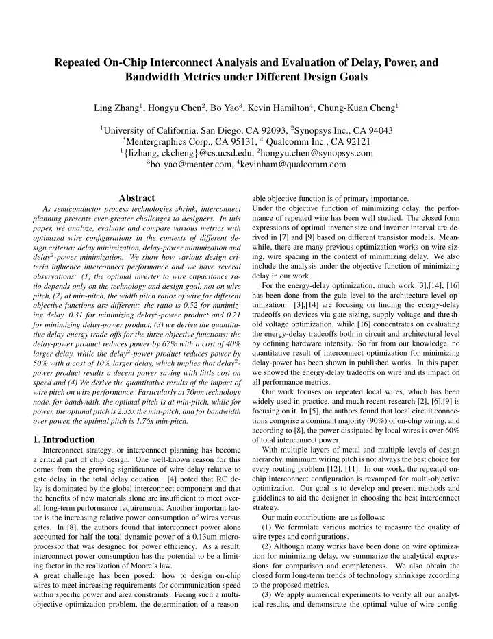
Repeated On-Chip Interconnect Analysis and Evaluation of Delay, Power, and Bandwidth Metrics under Different Design Goals Ling Zhang 1 , Hongyu Chen 2 , Bo Yao 3 , Kevin Hamilton 4 , Chung-Kuan Cheng 1 1 University of California, San Diego, CA
Repeated On-Chip Interconnect Analysis and Evaluation of Delay, Power, and Bandwidth Metrics under Different Design Goals Ling Zhang 1 , Hongyu Chen 2 , Bo Yao 3 , Kevin Hamilton 4 , Chung-Kuan Cheng 1 1 University of California, San Diego, CA 92093, 2 Synopsys Inc., CA 94043 3 Mentergraphics Corp., CA 95131, 4 Qualcomm Inc., CA 92121 1 { lizhang, ckcheng } @cs.ucsd.edu, 2 hongyu.chen@synopsys.com 3 bo yao@menter.com, 4 kevinham@qualcomm.com Abstract able objective function is of primary importance. Under the objective function of minimizing delay, the perfor- As semiconductor process technologies shrink, interconnect mance of repeated wire has been well studied. The closed form planning presents ever-greater challenges to designers. In this expressions of optimal inverter size and inverter interval are de- paper, we analyze, evaluate and compare various metrics with rived in [7] and [9] based on different transistor models. Mean- optimized wire configurations in the contexts of different de- while, there are many previous optimization works on wire siz- sign criteria: delay minimization, delay-power minimization and delay 2 -power minimization. We show how various design cri- ing, wire spacing in the context of minimizing delay. We also include the analysis under the objective function of minimizing teria influence interconnect performance and we have several delay in our work. observations: (1) the optimal inverter to wire capacitance ra- tio depends only on the technology and design goal, not on wire For the energy-delay optimization, much work [3],[14], [16] pitch, (2) at min-pitch, the width pitch ratios of wire for different has been done from the gate level to the architecture level op- objective functions are different: the ratio is 0.52 for minimiz- timization. [3],[14] are focusing on finding the energy-delay ing delay, 0.31 for minimizing delay 2 -power product and 0.21 tradeoffs on devices via gate sizing, supply voltage and thresh- for minimizing delay-power product, (3) we derive the quantita- old voltage optimization, while [16] concentrates on evaluating the energy-delay tradeoffs both in circuit and architectural level tive delay-energy trade-offs for the three objective functions: the by defining hardware intensity. So far from our knowledge, no delay-power product reduces power by 67% with a cost of 40% larger delay, while the delay 2 -power product reduces power by quantitative result of interconnect optimization for minimizing 50% with a cost of 10% larger delay, which implies that delay 2 - delay-power has been shown in published works. In this paper, we showed the energy-delay tradeoffs on wire and its impact on power product results a decent power saving with little cost on all performance metrics. speed and (4) We derive the quantitative results of the impact of Our work focuses on repeated local wires, which has been wire pitch on wire performance. Particularly at 70nm technology widely used in practice, and much recent research [2], [6],[9] is node, for bandwidth, the optimal pitch is at min-pitch, while for focusing on it. In [5], the authors found that local circuit connec- power, the optimal pitch is 2.35x the min-pitch, and for bandwidth tions comprise a dominant majority (90%) of on-chip wiring, and over power, the optimal pitch is 1.76x min-pitch. according to [8], the power dissipated by local wires is over 60% 1. Introduction of total interconnect power. With multiple layers of metal and multiple levels of design Interconnect strategy, or interconnect planning has become hierarchy, minimum wiring pitch is not always the best choice for a critical part of chip design. One well-known reason for this every routing problem [12], [11]. In our work, the repeated on- comes from the growing significance of wire delay relative to chip interconnect configuration is revamped for multi-objective gate delay in the total delay equation. [4] noted that RC de- lay is dominated by the global interconnect component and that optimization. Our goal is to develop and present methods and the benefits of new materials alone are insufficient to meet over- guidelines to aid the designer in choosing the best interconnect all long-term performance requirements. Another important fac- strategy. tor is the increasing relative power consumption of wires versus Our main contributions are as follows: gates. In [8], the authors found that interconnect power alone (1) We formulate various metrics to measure the quality of accounted for half the total dynamic power of a 0.13um micro- wire types and configurations. processor that was designed for power efficiency. As a result, (2) Although many works have been done on wire optimiza- interconnect power consumption has the potential to be a limit- tion for minimizing delay, we summarize the analytical expres- ing factor in the realization of Moore’s law. sions for comparison and completeness. We also obtain the A great challenge has been posed: how to design on-chip closed form long-term trends of technology shrinkage according wires to meet increasing requirements for communication speed to the proposed metrics. within specific power and area constraints. Facing such a multi- (3) We apply numerical experiments to verify all our analyt- objective optimization problem, the determination of a reason- ical results, and demonstrate the optimal value of wire config-
Recommend
More recommend
Explore More Topics
Stay informed with curated content and fresh updates.
