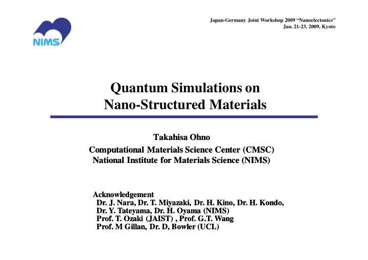
Quantum Simulations on Nano-Structured Materials Takahisa Ohno - PowerPoint PPT Presentation
Japan-Germany Joint Workshop 2009 Nanoelectonics Jan. 21-23, 2009, Kyoto Quantum Simulations on Nano-Structured Materials Takahisa Ohno Takahisa Ohno Computational Materials Science Center (CMSC) Computational Materials Science Center
Japan-Germany Joint Workshop 2009 “Nanoelectonics” Jan. 21-23, 2009, Kyoto Quantum Simulations on Nano-Structured Materials Takahisa Ohno Takahisa Ohno Computational Materials Science Center (CMSC) Computational Materials Science Center (CMSC) National Institute for Materials Science (NIMS) National Institute for Materials Science (NIMS) Acknowledgement Acknowledgement Dr. J. Nara, Dr. T. Miyazaki, Dr. H. Kino, Dr. H. Kondo, Dr. J. Nara, Dr. T. Miyazaki, Dr. H. Kino, Dr. H. Kondo, Dr. Y. Tateyama, Dr. H. Oyama (NIMS) Dr. Y. Tateyama, Dr. H. Oyama (NIMS) Prof. T. Ozaki (JAIST) , Prof. G.T. Wang Prof. T. Ozaki (JAIST) , Prof. G.T. Wang Prof. M Gillan, Dr. D, Bowler (UCL) Prof. M Gillan, Dr. D, Bowler (UCL)
Nano-structured materials To understand their formation processes & properties/functions at the atomistic level, FP simulation methods based on DFT are an ideal tool. Surface dynamics (DFT/ Hybrid) Surface dynamics (DFT/ Hybrid) (i) Diffusion of (i) Diffusion of F on Si(111) F on Si(111) : Si Si- -F complex diffusion F complex diffusion (ii) Adsorption of (ii) Adsorption of O2 on Si(001) O2 on Si(001) : : Energy dissipation Energy dissipation (iii) Atomic structure of AFM tip apex (iii) Atomic structure of AFM tip apex Large nano Large nano- -structured systems structured systems (i) PW electronic structure codes (i) PW electronic structure codes : : shallow impurity in Si shallow impurity in Si (ii) Linear scaling algorithms: (ii) Linear scaling algorithms: (a) Surface nano (a) Surface nano- -structures; structures; Ge cluster on Si(001) Ge cluster on Si(001) (b) Bio- (b) Bio -molecules: molecules: DNA DNA Transport through molecular junctions (NEGF) Transport through molecular junctions (NEGF) (i) p (i) p- -stacked systems: styrene wires on H/Si(001) stacked systems: styrene wires on H/Si(001) (ii) Molecular sensors: (ii) Molecular sensors: iron iron- -porphyrin porphyrin (iii) Molecular switch: biphenyl dithiol Photochemical reaction (RTP- Photochemical reaction (RTP -TDDFT) TDDFT) (i) Photoisomerization: azobenzene (i) Photoisomerization: azobenzene Redox reaction Redox reaction - (aq) + H O(l) + e - -- - (aq) RuO 4- RuO (aq) + H 2 O(l) + e --> [RuO > [RuO 3 (OH) (OH) 2 ] 2- (aq) (i) RuO4: (i) RuO4: 平成 21 年 2 月 25 日 2
Diffusion of F on Si(111) Diffusion of F on Si(111) F diffusion on Si(111) F diffusion on Si(111)- -(7x7) (7x7) -4 -4 done by Prof. Sakurai’s group done by Prof. Sakurai’s group F蒸着表面 F F+Si 蒸着表面 Ea=1.3 eV Ea=1.3 eV -5 -5 F+Si Si adatom Si adatom @300 ℃ @300 adsorbed F adsorbed F -6 -6 ln κ ln κ F: ΘF= 0.012ML, T = 235~350℃ -7 -7 F+Si:ΘF= 0.013ML, ΘSi=0.005ML, -8 -8 T = 258~325℃ The deposition of excess Si adsatoms The deposition of excess Si adsatoms After 90 sec. After 90 sec. on Si(111) enhances the diffusion ! on Si(111) enhances the diffusion ! -9 -9 -10 -10 20 20 19 19 21 21 22 22 24 24 Si(001) Si(001) Si(111) Si(111) 18 18 23 23 1/kT 1/kT n.n. Si- n.n. Si -Si Si 3.8 A 3.8 A 4.5 A 4.5 A Ediff Ediff 1.8 eV 1.8 eV 1.3 eV 1.3 eV The F diffusion is assisted by excess Si atoms. The F diffusion is assisted by excess Si atoms. Surface diffusion which depends on diffusing Si density has not been observed so far. Surface diffusion which depends on diffusing Si density has not been observed so far. The diffusion mechanism in atomic scale is not clarified. The diffusion mechanism in atomic scale is not clarified. 平成 21 年 2 月 25 日 3
Diffusion of F on Si(111) Diffusion of F on Si(111) Y. Fujikawa, et. al. : J. Chem. Phys. 129, 234710 (2008) (1) Single F atom hopping (1) Single F atom hopping Ea=2.32 eV Ea=2.32 eV Si(111) Si(111)- -(5x5) (5x5) F F Si Si Si Ea > 2eV Ea > 2eV (2) Si assisted F diffusion (2) Si assisted F diffusion F F Si Si F Si Si Si Adsorbed F Adsorbed F Adsorbed Si Adsorbed Si (3) Si- (3) Si -F complex diffusion F complex diffusion Ea=1.34 eV Ea=1.34 eV Top view Top view Top view Top view F F Si Si Si Side view Side view Side view Side view SiF complex diffusion model can explain experiments. SiF complex diffusion model can explain experiments. 平成 21 年 2 月 25 日 4
Diffusion of Si- Diffusion of Si -F complex F complex ●: F ●: excessSi ● : adatom (complex) ● : adatom ●: restatom SiF +0.03 +0.32 +0.27 +0.36 +0.49 +0.41 +0.41 +0.52 +1.18 a b c d e f g h i ( 単位 : eV) 1.5 +1.10 i +1.04 +0.87 Energy (eV) +1.34 +0.82 1.0 +0.70 +0.56 +0.43 0.5 e h g d f a b c 0.0 平成 21 年 2 月 25 日 5
Adsorption of O2 on Si(111): hybrid method Adsorption of O2 on Si(111): hybrid method How the adsorption/reaction energy is used for the formation of the final adsorption geometry. How the adsorption/reaction energy is used for the formation of the final adsorption geometry. FP/TB/MM hybrid calculations FP/TB/MM hybrid calculations ゲート ゲート ソース ソース ドレイン ドレイン Si/SiO Si/SiO 2 Si Si 基板 基板 FP FP O 2 [001] [001] Si Si Si Si TB TB 65 atomic layers atomic layers MM MM It is important to deal with the dissipation It is important to deal with the dissipation of the released energy properly. of the released energy properly. Back- Back -bond oxidation bond oxidation 平成 21 年 2 月 25 日 N. Takahashi, T. Ohno: Surf. Sci. 602, 768 (2008) 6
AFM tip apex: hybrid method AFM tip apex: hybrid method How does the atomic protrusion exists at the AFT tip apex? How does the atomic protrusion exists at the AFT tip apex? ■ AFM AFM Nakamura, Takahashi, Uda, and Ohno: PRL 97, 086103 (2006) Nakamura, Takahashi, Uda, and Ohno: PRL 97, 086103 (2006) image (〜 μ m) SEM SEM image Hybrid calculations Hybrid calculations (〜10nm) FP FP ~5000 Si ~5000 Si atoms atoms TB TB MM MM AFM performance depends on the atomic structure of the tip. AFM performance depends on the atomic structure of the tip. By the present techniques, the atomic geometry of the very end By the present techniques, the atomic geometry of the very end of the tip is practically impossible to control. of the tip is practically impossible to control. But, we can obtain AFM images with atomic resolution. But, we can obtain AFM images with atomic resolution. Atomic protrusion Atomic protrusion B A @300K @300K 平成 21 年 2 月 25 日 7
Shallow Impurity in Si Shallow Impurity in Si Conventional PW electronic structure code parallelized for Earth Simulator ■ As shallow impurity in Si As shallow impurity in Si Si 10647 As Impurity level Gate e - e - e - e - Donor levels Drai Source n 2 nm As As atom atom Wavefunction Wavefunction PHASE performance on ES PHASE performance on ES Theoretical peak performance 16.2 Tflop/s (50%) Concentration ~ 10 Concentration 10 20 20 /cm /cm 3 *SC07: Gordon Bell prize finalist *SC07: Gordon Bell prize finalist (2007/11/14) (2007/11/14) 平成 21 年 2 月 25 日 8
Linear Linear- -Scaling DFT Calculations Scaling DFT Calculations Order Order- -N code: CONQUEST N code: CONQUEST 平成 21 年 2 月 25 日 9
First- First -Principles Order Principles Order- -N methods N methods First- First -Principles Order Principles Order- -N methods N methods Scaling linearly with N Scaling linearly with N Bulk Si (4096 Bulk Si (4096- -12288 atoms) 12288 atoms) � CONQUEST CONQUEST : density matrix density matrix 300.0 300.0 In collaboration with Prof. Gillan (UCL) In collaboration with Prof. Gillan (UCL) CPU time (sec) (sec) limited β -version released on limited version released on May 16th, 2007 May 16th, 2007 CPU time Application to nano- Application to nano -materials materials � Quantum Quantum- -dots dots � Bio Bio-materials materials 14000 14000 Numer of atoms Numer of atoms DNA DNA Ge clusters on Si(001) Ge clusters on Si(001) Bio- Bio -materials materials 平成 21 年 2 月 25 日 10
Recommend
More recommend
Explore More Topics
Stay informed with curated content and fresh updates.
