Ultra High-Speed InGaAs Nano-HEMTs 2003. 10. 14 Kwang-Seok Seo - PDF document
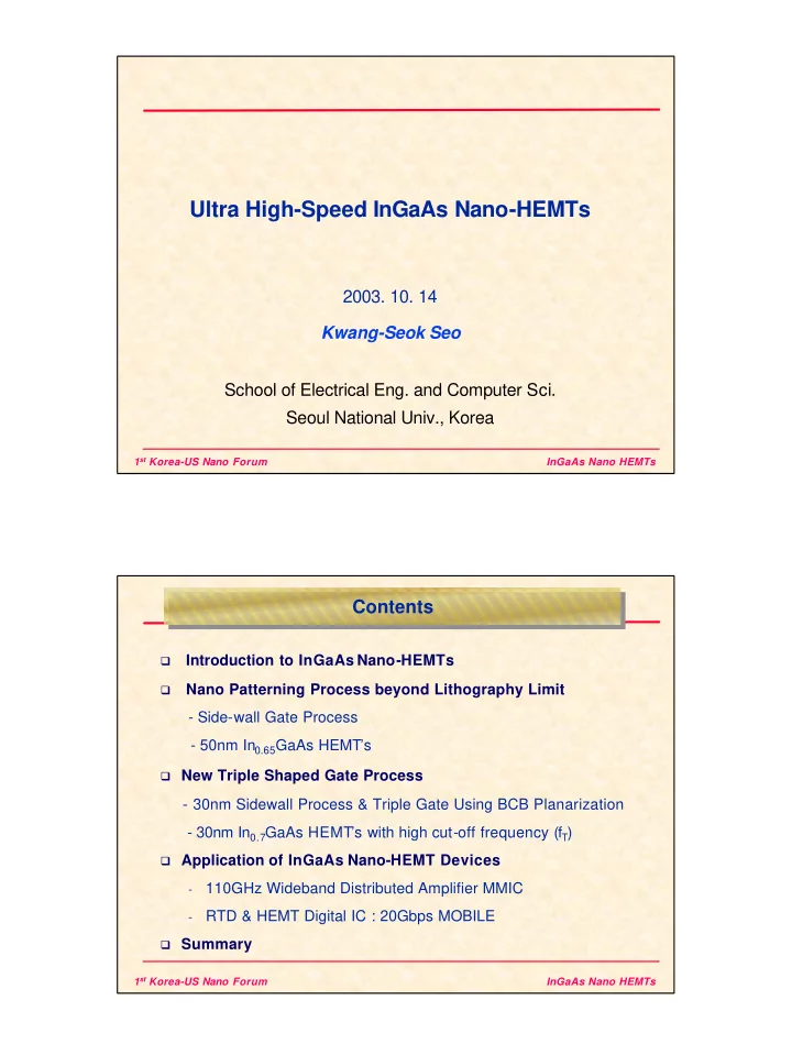
Ultra High-Speed InGaAs Nano-HEMTs 2003. 10. 14 Kwang-Seok Seo School of Electrical Eng. and Computer Sci. Seoul National Univ., Korea 1 st Korea-US Nano Forum InGaAs Nano HEMTs Contents Contents Introduction to InGaAs Nano-HEMTs Nano
Ultra High-Speed InGaAs Nano-HEMTs 2003. 10. 14 Kwang-Seok Seo School of Electrical Eng. and Computer Sci. Seoul National Univ., Korea 1 st Korea-US Nano Forum InGaAs Nano HEMTs Contents Contents Introduction to InGaAs Nano-HEMTs � Nano Patterning Process beyond Lithography Limit � - Side-wall Gate Process - 50nm In 0.65 GaAs HEMT’s � New Triple Shaped Gate Process - 30nm Sidewall Process & Triple Gate Using BCB Planarization - 30nm In 0.7 GaAs HEMT’s with high cut-off frequency (f T ) � Application of InGaAs Nano-HEMT Devices 110GHz Wideband Distributed Amplifier MMIC - RTD & HEMT Digital IC : 20Gbps MOBILE - � Summary 1 st Korea-US Nano Forum InGaAs Nano HEMTs
Millimeter-Wave/Tera-Hz Technology Millimeter-Wave/Tera-Hz Technology � Broad Bandwidth � High Speed Data Communication � Small Size Antenna � Mobile Communication/Automobile Radar � High Resolution Imaging � Biomedical Imaging ( > 100GHz) Millimeter wave Auto. Radar Demands for High Frequency/High Performance Devices & Circuits � Nano-technology enhances the speed of devices & circuits. (due to the reduction of carrier transit time) 1 st Korea-US Nano Forum InGaAs Nano HEMTs State-of-the-art InGaAs Nano-HEMT’s State-of-the-art InGaAs Nano-HEMT’s n + InGaAs InP InAlAs In 0.7 GaAs CRL- Fujitsu Group’s Work (02,EDL) Gate Length = 25nm f T = 562GHz In 0.7 GaAs Channel (World Record) (with v peak ~ 3.4x10 7 cm/ s) * Fabricated by the state-of-the-art E-beam lithography system 1 st Korea-US Nano Forum InGaAs Nano HEMTs
How to improve f T of Nano-HEMT’s ? How to improve f T of Nano-HEMT’s ? � L g Reduction : L g < 30nm � Strained Channel ( I n x GaAs) R g T- Gate - I ndium Content > 0.7 Metal for Higher v average C par � Structure for Small Parasitics SiO 2 / SiN - Reduction of L g,2nd (< 100nm) x - I ncrease of Height (> 150nm) Recess � f T Enhancement L g � Two-Step Recess Etching I nGaAs/ I nAlAsEpi-Wafer - Damage-Free Condition � Structural Stability < Cross-section of Nano-HEMT’s > - Wide T-Gate : Small R g 1 st Korea-US Nano Forum InGaAs Nano HEMTs Nano Patterning beyond Lithography Limit Nano Patterning beyond Lithography Limit ♦ PR Trimming By Plasma Asing ♦ Side-wall Process Ashing Etch - backed dielectric Photo - resist Dielectric Dielectric Substrate Substrate ♦ RIE Lag Effect ♦ Photo-resist Flow Process Photo - resist Photo - resist Photo - resist Photo - resist Dielectric Dielectric Substrate Substrate 1 st Korea-US Nano Forum InGaAs Nano HEMTs
Low-Damage & Reproducible Side-wall Process Low-Damage & Reproducible Side-wall Process 100 nm Oxide � Two-step Dielectric Etch-back 100 nm - CF 4 / O 2 Mixture : Etching SiO 2 SiN x - SF 6 / Ar Mixture : Etching the residual SiN x < 1 st Line Definition & Re -depo. > 1) Lower Damage than that of other gas Oxide 2) Etch Selectivity of SiN x over SiO 2 SiN x - Typical Selectivity = ~ 20 < Oxide Etch-back by CF 4 Plasma > � L g,final : I nsensitive to over-etch cond. � Low-Damaged & Reproducible Oxide L g,final � L g,final = ~ L g,initial / 2 SiN x < SiN x Etch-back by SF 6 Plasma > 1 st Korea-US Nano Forum InGaAs Nano HEMTs Sidewall Process Results : 50nm Line Sidewall Process Results : 50nm Line PMMA SiO 2 SiN x L g = 100nm SiN x (a) 1 st Gate Definition (c) Etch-Back : On Etching Sidewall Void L g = 50nm (b) SiO 2 Re-deposition (d) Final Sidewall Gate 1 st Korea-US Nano Forum InGaAs Nano HEMTs
50nm Double Decked T- Gate Fabrication 50nm Double Decked T- Gate Fabrication PMMA T-gate defined Photo by EBMF 10.5 copolymer T -Gate Metal -Resist C par_1 PMMA(200nm) C par_1 Gate foot defined by SiN x (100nm) Dielectric Side-wall Process C par_2 C par_2 ← Reduction of C parasitics for Higher f T 200nm 50nm 1 st Korea-US Nano Forum InGaAs Nano HEMTs Epitaxial Structures for Nano-HEMT Fabrication Epitaxial Structures for Nano-HEMT Fabrication < Epitaxial Structure > < Cross-Section of Nano-HEMT > Schottky 19 n+ InGaAs Cap. 1X10 20nm On InAlAs δ -doping i InP Etch-stopper 4nm Passivation Layer i In AlAs Barrier 8nm 0.52 Selective i In GaAs Channel 10nm Wet Etch 0.65 Spacer i In GaAs Channel 10nm Ar-RIE with 0.53 In 0.53 GaAs Low Damage i In AlAs Buffer 500nm InPEtch-stopper 0.52 In 0.52 AlAs Barrier Si Delta-Doping In 0.52 AlAs Spacer S.I. InP Substrate In 0.65 GaAs Strained Channel In 0.53 GaAs Pre-Channel n s =3x10 12 /cm 2 , µ n,hall =10,300cm 2 /V-s 1 st Korea-US Nano Forum InGaAs Nano HEMTs
50nm InGaAs Nano-HEMT : DC Characteristics 50nm InGaAs Nano-HEMT : DC Characteristics < L g = 50nm & 65% Strained InGaAs Channel > � V th = -0.6V & G m,max = 1.07S/mm @ V ds = 1.0V 1 st Korea-US Nano Forum InGaAs Nano HEMTs 50nm InGaAs Nano-HEMT: Microwave Characteristics 50nm InGaAs Nano-HEMT: Microwave Characteristics - Bias Point : Maximum Transconductance Condition - f T = 305GHz ⇒ f T = 305 GHz & f max = 302GHz 1 st Korea-US Nano Forum InGaAs Nano HEMTs
InGaAs Nano-HEMT’s : Metal Filling Issue InGaAs Nano-HEMT’s : Metal Filling Issue Metal High Performance Nano- HEMTs SiO 2 � L g � , T-Gate Aspect Ratio � (For Small C parasitics ) SiN x � metal filling of fine line with high A-R needed. Epi - Structure < Gate Filling By E-Beam Evaporation> < Gate Filling By W-Sputtering> Only 60nm Filling W= 150nm L g = 40nm H= 200nm W Filling Aspect Ratio (H/ L g ) = 5 Good Gate Metal Filling Not Filled After 50nm Evaporation W : Good Thermal Reliability 1 st Korea-US Nano Forum InGaAs Nano HEMTs T-Gate Process for 30nm InGaAs HEMT’s T-Gate Process for 30nm InGaAs HEMT’s High Temp. Sputter : Problem in Lift-off � Metal Etch Process BCB Planarization Ti/Au Ti/Au Dielectric Ti/Au BCB PMMA PMMA W Ti/Au Dielectric Dielectric Tusten (W) Good Filling Epi-wafer Dielectric Dielectric High Temp. Epi-wafer Sputter BCB Etch-Back Ti/Au & Head Litho. Ti/ Au Lift -off & W-Etch Ti/Au Ti/Au BCB W W Dielectric Dielectric Dielectric Dielectric Epi-wafer Epi-wafer < New Triple Gate Process Using High Temp. Sputter & BCB Planarization > 1 st Korea-US Nano Forum InGaAs Nano HEMTs
30nm In 0.7 GaAs HEMT’s : DC I-V 30nm In 0.7 GaAs HEMT’s : DC I-V < L side-etch = 50nm & No I nP Etch > < L side-etch = 50nm & I nP Etch> V g s : 0 . 2 V t o - 1 . 2 V i n - 0 . 2 V s t e p V g s : 0 . 3 V t o - 0 . 5 V i n - 0 . 1 V s t e p 1 2 0 0 8 0 0 Schottky on I nP/ I nAlAs Schottky on I nAlAs (10nm ) mm] mm] (4/ 10nm) / / mA mA 6 0 0 4 0 0 [ [ s s d d I I 0 0 0 . 0 1 . 0 2 . 0 0 . 0 1 . 0 2 . 0 V d s [ V ] V d s [ V ] = > V th = -0.85V & G m,max = 1.75S/ mm = > V th = -0.3V & G m,max = 1.69S/ mm = > High Short channel effect = > Low Short channel effect G m / G ds = 3.89 @ G m,max Bias Point G m / G ds = 10.6 @ G m,max Bias Point 1 st Korea-US Nano Forum InGaAs Nano HEMTs RF Characteristics of 30nm In 0.7 GaAs HEMT’s RF Characteristics of 30nm In 0.7 GaAs HEMT’s < Best f T Charateristics > < f T versus Gate Bias > � f T = 421GHz at V gs / V ds = -0.15 / 1.05V 1 st Korea-US Nano Forum InGaAs Nano HEMTs
Performances of SNU InP Nano-HEMT’s Performances of SNU InP Nano-HEMT’s < f T versus L g > 1 ⋅ v = π f sat T 2 L G , eff L G reduction ⇒ decrease of τ transit ⇒ increase of f T SNU I nGaAs Nano-HEMT ( 2 0 (2003) 0 2 ) � f T = 250GHz for L g =60nm ( 2 � f T = 305GHz for L g =50nm 0 0 1 ) � f T = 371GHz for L g =40nm � f T = 421GHz for L g =30nm 1 st Korea-US Nano Forum InGaAs Nano HEMTs Over 110GHz Broadband Distributed Amplifier Over 110GHz Broadband Distributed Amplifier Output+ V D - Chip size:1.5X0.7mm 2 - Output+ V D Unit cell I nput+ V G1 V G2 < Schematic of distributed amplifier > V G2 I nput+ V G1 < Photograph of distributed amplifier > • Broadband distributed amplifier with 60nm InGaAs Nano-HEMT • The average gain at 1~110GHz is about 6.6 dB. • S 11 < -11 dB, S 22 < -4 dB < Measured S-parameter > 1 st Korea-US Nano Forum InGaAs Nano HEMTs
RTD & HEMT Digital IC – 20Gbps MOBILE RTD & HEMT Digital IC – 20Gbps MOBILE RTD HEMT BCB Current Density(kA/cm 2 ) 1000 PVCR ~ 9 G m ~ 1.1 S / mm 100 J peak > 5.5x10 4 A/cm 2 800 f T = 180GHz 50 Chip size : 0.75X0.68mm 2 I DS [mA/mm] 600 0 400 250 mV P-P -50 200 -100 0 50 -1.0 -0.5 0.0 0.5 1. 0.0 0.5 1.0 1.5 psec 0 Voltage [V] V S [V] D < RTD I-V Curve > < HEMT I-V Curve : L g =100nm > 20Gbps 2 31 -1 PRBS Output Signal 1 st Korea-US Nano Forum InGaAs Nano HEMTs Summary Summary � Nano Patterning Method beyond Lithography Limit - Sidewall Process / Resist Flowing / Sloped Etch By RIE-Lag � 30nm In 0.7 GaAs Nano-HEMT - Sidewall Process + Triple Gate Process Using BCB Planarization - G m,max = 1.75S/mm & f T = 421GHz � Application of Developed InGaAs Nano-HEMT Device - 110GHz Wideband Distributed Amplifier (DA) MMIC : B-W > 110GHz - MOBILE IC based on RTD & HEMT Integration > 20Gbps � In future, the high speed characteristics of InGaAs nano-HEMT are to be enhanced with nano-technology [reduction of gate length], and ultra-high-speed ICs are to be implemented with nano-HEMTs. 1 st Korea-US Nano Forum InGaAs Nano HEMTs
Recommend
More recommend
Explore More Topics
Stay informed with curated content and fresh updates.
