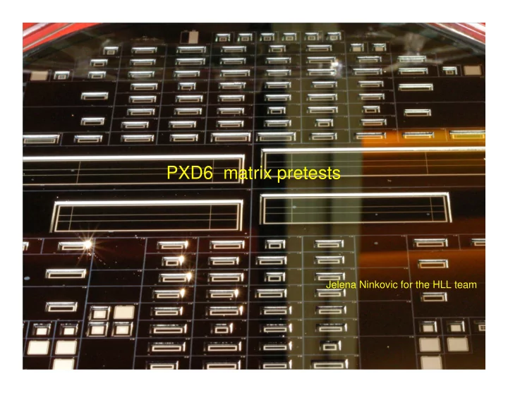

PXD6 matrix pretests Jelena Ninkovic for the HLL team
PXD6 Production Status Production was split before the 1 st metal layer - reduces risk - accelerates finalization Status of the first batch (4 wafers: 3 SOI+1ref): metal_2 • Processing finished oxide • Yield measured on the wafer level metal_1 polySi_2 polySi_1 n+ p+ deep n • 3 wafers (2SOI+1ref) cut deep p • One wafer repaired n bulk Status of the second batch (4 wafers: 3 SOI+1ref): • Processing finished • Yield measured on the wafer level • 2 wafers repaired- matrix pretests ongoing Status of the third batch (2 SOI wafers with DHP footprint): • Processing done till Cu (last layer BCB) • Yield measured on the wafer level • Matrix pretests ongoing Jelena Ninkovic 2 EVO meeting 14.12.2011
Automated pretesting of matrices 4 rows of readout pads For small matrices each pad has 16 transistors connected (128drains x 16gates) 16 0 3 • Keep all transistors ON and measure I on each readout pad • Numbers in the table show number of transistors are connected (max number 16) • Automatic measurement procedure was developed to measure yield of matrices before bonding Jelena Ninkovic 3 EVO meeting 14.12.2011
Results of the pretests on Batch 1 before repair 0 transistors connected 16 transistors connected Jelena Ninkovic 4 EVO meeting 14.12.2011
Cause of a problem Effect present only on wafers that have seen back side processing Analysis of process steps on the back side Photolithography on the backside: Front sides of the wafers were never protected during the photolithography steps on the back side During this process step wafer goes into developer For reference wafers this step takes ~30s whereas for etched SOI wafers the thickness of photoresists requires much longer times (~15min) Developer was slowly etching Aluminum on the non protected side … Jelena Ninkovic 5 EVO meeting 14.12.2011
Can we repair it somehow ?? Deposit 3 rd Al layer and structure it on top of an already existing extreme topology Metal 3 metal_2 oxide metal_1 polySi_2 polySi_1 n+ p+ deep n deep p n bulk Jelena Ninkovic 6 EVO meeting 14.12.2011
Problems during the repair Al 2 Al2 Al 1 Al 1 Poly Si Poly Si Jelena Ninkovic 7 EVO meeting 14.12.2011
Matrix pretests Batch 1 after repair 0 transistors connected 16 transistors connected 32 transistors connected Jelena Ninkovic 8 EVO meeting 14.12.2011
Matrix pretests Batch 2 after repair Finished yesterday Yield of the measured matrices 0 transistors >99% connected 16 transistors connected 32 transistors connected Jelena Ninkovic 9 EVO meeting 14.12.2011
Matrix pretests Batch 3 Yield of all up to now measured matrices >98% 0 transistors connected 16 transistors connected Jelena Ninkovic 10 EVO meeting 14.12.2011
Thank you for your attention! Jelena Ninkovic 11 EVO meeting 14.12.2011
Recommend
More recommend