PROCESS STEPS Application Fields Portable Electronics (PC, PDA, - - PowerPoint PPT Presentation
PROCESS STEPS Application Fields Portable Electronics (PC, PDA, Wireless) IC Cost (Packaging and Cooling) Reliability (Electromigration, Latch- up) Signal Integrity (Switching Noise, DC Voltage Drop) Thermal Design
PROCESS STEPS
Application Fields
- Portable Electronics (PC, PDA,
Wireless)
- IC Cost (Packaging and Cooling)
- Reliability (Electromigration, Latch-
up)
- Signal Integrity (Switching Noise,
DC Voltage Drop)
- Thermal Design
- Ultra-low-power applications
- Space missions (miniaturized
satellites)
Arun N. Chandorkar, IIT Bombay
Different Constraints for Different Application Fields
- Portable devices: Battery life-time
- Telecom and military: Reliability
(reduced power decreases electromigration, hence increases reliability)
- High volume products: Unit cost
(reduced power decreases packaging cost)
Arun N. Chandorkar, IIT Bombay
Is Transistor a Good Switch?
On I = ∞ I = 0 Off I = 0 I = 0 I ≠ 0 I = 1ma/u I ≠ 0 I ≠ 0 Sub-threshold Leakage
4 5
MOSFET Scaling Problem: Saturation of IDsat
200 400 600 800
0.1 0.2 0.25 0.3 0.4 0.6 0.8 1.0
NMOS PMOS IDsat (A/m) (drive current) Channel Length (µm)
Data from IBM, TI, Intel, AMD, Motorola and
Lucent
Low OFF current desirable
0.4 0.8 1.2 1990 1995 2000 2005 1 10 Supply Voltage (V) Drive Current (mA/µm)
Changhoon Choi, PhD Thesis, Stanford Univ., 2002
Constant OFF current Limit Relaxed OFF current Limit
Source: Intel
Low Vt High Vt
IOFF,hig h Vt IOFF,low Vt
Vg log Id
Leakage Power
0% 10% 20% 30% 40% 50% 1.5 0.7 0.35 0.18 0.09 0.045
Technology (µ) Leakage Power (% of Total)
Must stop at 50%
Leakage power limits Vt scaling
- A. Grove, IEDM 2002
INTEL
Subthreshold Leakage (A/µµ) Operation Frequency (a.u.) e) 100 10 1
Source: 2007 ITRS Winter Public Conf.
The limit is deferent depending on application
Gate Oxide is Near Limit
Poly Si Gate Electrode Si Substrate 1.5 nm Gate Oxide
70 nm Si3N4 CoSi2
130nm Transistor
Will high K happen? Would you count on it?
INTEL
- P. P. Gelsinger, “Microprocessor for the New Millennium: Challenges,
Opportunities, and New Frontiers,” Dig. Tech. 2001 ISSCC, San Francisco, pp.22-23, February, 2001
Microprocessors Trend expected in 2001
Today: 2002 (Intel) Lg sub-70 nm Tox 1.4 nm f 2.53 GHz P several 10 W N 50 M Heat Generation 2002 10W/cm2 Hot Plate 2006 100W/cm2 Surface of Nuclear Reactor 2010 1000W/cm2 Rocket Nozzle 2016 10000W/cm2 Sun Surface 2008 (Intel) Lg sub-25 nm Tox 0.7 nm f 30 GHz P 10 kW N 1.8B MIPS 1M MIPS (TIPS) Power Increase
- Tr. Number increase
Clock Frequency increase Cause Solution: Low supply Voltage Past: 1972 (Intel) Lg 10,000 nm Tox 1200 nm f 0.00075 GHz P a few 100 mW N 2.25k Heat generation increase
20 40 60 80 100 120
- 39.71
- 25.27
- 10.83
3.61 18.05 32.49
∆VTn(mv) # of Chips
~30mV
VT Distribution
0.18 micron ~1000 samples
Low Freq Low Isb High Freq Medium Isb High Freq High Isb
INTEL
Impact on Path Delays
Path Delay
Path delay variability due to variations in Vdd, Vt, and Temp Impacts individual circuit performance and power Optimize each circuit for full chip objectives
Delay Probability
Objective: full chip performance, power, and yield Multivariable optimization of individual circuit—Vdd, Vt, size
Towards the end of the (ITRS) Roadmap
- Feature sizes approach
single-digit nanometers
- Physical and economic
limits to scaling
Red Brick Wall!
New Technologies
– Chemically Assembled Electronic Nanotech. (CAEN) – Extreme Ultraviolet (EUV) Lithography
Qi Xinag, ECS 2004, AMD
Gate Oxd Channel
Electron wave length 10 nm Channel length?
Scaling limit?
Hiroshi Iwai
5 nm gate length CMOS
- H. Wakabayashi
et.al, NEC IEDM, 2003
Length of 18 Si atoms
Is a Real Nano Device!!
5 nm
Hiroshi Iwai
Electron wave length 10 nm Tunneling distance 3 nm Atom distance 0.3 nm
Prediction at present
Practical limit because of off-leakage between S and D?
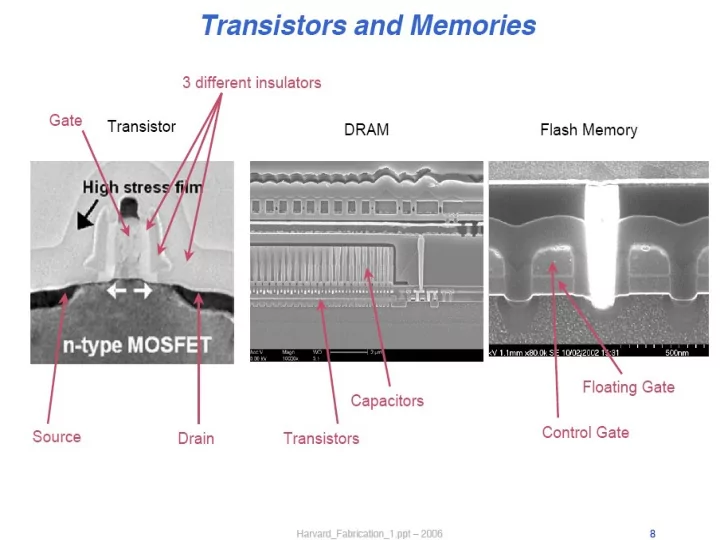
Lg = 5 nm?
MOSFET operation
Lg = 2 ~ 1.5 nm?
But, no one knows future!
Gate length
Prediction now!
By Robert Chau, IWGI 2003 0.8 nm Gate Oxide Thickness MOSFETs operates 0.8 nm: Distance of 3 Si atoms!!
So, we are now in the limitation Of Scaling? Do you believe this or do not????
There is a solution! To use high-k dielectrics
Thin gate SiO2 Thick gate high-k dielectrics Almost the same electric characteristics However, very difficult and big challenge! Remember MOSFET had not been realized without Si/SiO2!
K: Dielectric Constant
Thick Small leakage Current
- R. Hauser, IEDM Short Course, 1999
Hubbard and Schlom, J Mater Res 11 2757 (1996)
- Gas or liquid
at 1000 K
- H
○ Radio active He
- ● ● ● ● ●
Li B e
B C N O F Ne ①
- ● ● ●
NaMg
Al Si P
S Cl Ar ② ① ① ① ① ① ① ① ① ① ① ● ● ● ● K Ca Sc Ti V Cr Mn Fc Co Ni Cu Zn Ga Ge As Se Br Kr
- ① ①
① ① ① ● ① ① ① ① ① ● ● Rh Sr Y Zr Nb Mo Tc Ru Rb Pd Ag Cd In Sn Sb Te I Xe
- ③
① ① ① ① ① ● ● ● ● ① ① ○ ○ ○ Cs Ba ★ Hf Ta W Re Os Ir Pt Au Hg Tl Pb Bi Po At Rn ○ ○ ○ ○ ○ ○ ○ ○ Fr Ra ☆ Rf Ha Sg Ns Hs Mt ○
LaCe Pr Nd PmSmEuGdTbDyHo Er TmY bLu
○ ○ ○ ○ ○ ○ ○ ○ ○ ○ ○ ○ ○ ○ ○ Ac Th Pa U Np Pu AmCm Bk Cf Es Fm Md No Lr ★ ☆
Candidates
- ●
Na
Al Si P
S Cl Ar ② ① ① ① ① ① ① ① ① ① ● ● ● ● K
Sc Ti
V Cr Mn Fc Co Ni Cu Zn Ga Ge As Se Br Kr
- ① ①
① ① ① ● ① ① ○ ○ ○ ○ ○ ○ Ac Th Pa U Np Pu AmCm Bk Cf Es Fm Md No Lr ★ ☆
② ③
Unstable at Si interface
Si + MOX M + SiO2
①
Si + MOX MSiX + SiO2 Si + MOX M + MSiXOY
Choice of High-k elements for oxide
HfO2 based dielectrics are selected as the first generation materials, because of their merit in 1) band-offset, 2) dielectric constant 3) thermal stability La2O3 based dielectrics are thought to be the next generation materials, which may not need a thicker interfacial layer
Intel’s announcement, January 26, 2007, and IEDM Dec 2010 Hafnium-based high-k material by ALD: EOT= 1nm Specific gate metals ( Intel’s trade secret) Different Metals for NMOS and PMOS Use of 193nm dry lithography From 45 nm to 32 nm Tech. Tr density: 2 times increase Tr witching power: 30% reduction Tr witching speed: 20% improvement S-D leakage power: 5 times reduction Gate oxide leakage: 10 times reduction 45nm processors (Core™2 family processors "Penryn") running Windows* Vista*, Linux* etc. 11nm production in the First half of 2015 or Early 2016.
PMOS
High-k gate insulator MOSFETs for Intel: EOT=1nm EOT: Equivalent Oxide Thickness
EOT = 0.48 nm
Transistor with La2O3 Gate Insulator
TIT results
Time
Conclusion: Technology Progression
Well doping channel Depletion layer isolation haloBulk CMOS
Si0.8Ge0.2 Si Si (tensile) Si1-xGexStrained Si High k gate dielectric Metal gate 3D ICs
2 nm
Cu interconnect Low-k ILD FD SOI CMOS
channel depletion layer isolation buried oxide raised source/drainOptical interconnect Molecular device Detectors, lasers, modulators, waveguides Spin device
B + =
Ge on Si hetroepitaxy Ge on Insulator Wafer bonding Crystallization Nanowires Ge/Si Heterostrcture Double-Gate CMOS Nanowire Single e transistor Nanotube
Feature Size
Carbon Nanotubes
Graphene Device
Graphene Device Electronics(??)
- A study of how electrons behave in
circuitry made from ultrathin layers of graphite – known as graphene – suggests the material could provide the foundation for a new generation of nanometer scale devices that manipulate electrons as waves – much like photonic systems control light waves.
Graphene 3D structure and Band Diagram
In 2004 two scientists, Andre Geim and Konstantin Novoselov, both of whom would later receive the Nobel Prize for their work In preparation of Graphene
Graphene based (2D Material)Transistor
Standard NMOSFET Graphene Based Transistor
Graphene transistor and new possible Ballistic Device
Tunneling Effect
Coulomb Blockade
- a Coulomb blockade
is the increased resistance at small bias voltage of an electronic device comprising at lease
- ne low-capacitance
tunnel junction.
Bottom-Up
Self Assembly
- Applicatoins: solar cell, light-emitting
diodes, capsule in drug delivery system
Chemical Colloidal Method
Lithography and Etching
- Lithography: electron beam, ion beam,
nanoimprint, dip pen nanolithography
- Etching: wet etching, dry etching, plasma,
implantation, photo etching
Split-gate Approach
- Use additional voltage to create 2
dimensional confinements to control the shape and size of the quantum dot’s gate.
- It’s a combination of e beam lithography,
evaporation, lift off, contact annealing
Limitations of CMOS in ~ 10 years
- Fundamental physical limit
- 8 electron per bit
(today 1000 e/bit)
- Manufacturing cost
- $50 Billion/FAB