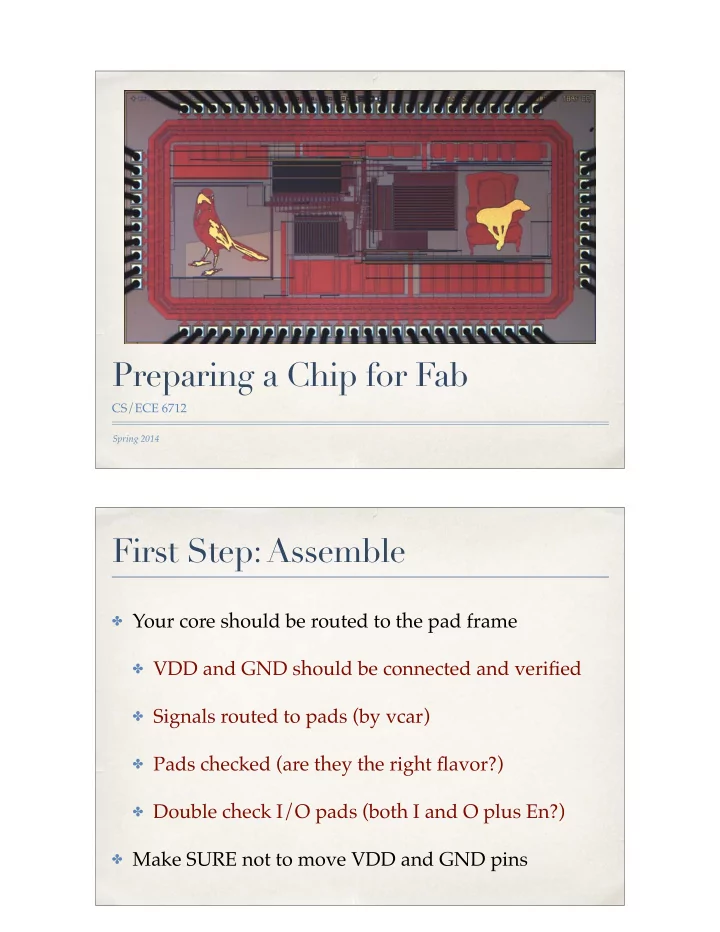
Preparing a Chip for Fab CS/ECE 6712 Spring 2014 First Step: - PDF document
Preparing a Chip for Fab CS/ECE 6712 Spring 2014 First Step: Assemble Your core should be routed to the pad frame VDD and GND should be connected and verified Signals routed to pads (by vcar) Pads checked (are they the
Preparing a Chip for Fab CS/ECE 6712 Spring 2014 First Step: Assemble ✤ Your core should be routed to the pad frame � ✤ VDD and GND should be connected and verified � ✤ Signals routed to pads (by vcar) � ✤ Pads checked (are they the right flavor?) � ✤ Double check I/O pads (both I and O plus En?) � ✤ Make SURE not to move VDD and GND pins
Step 2: DRC/EXT/LVS Step 2: DRC/EXT/LVS
Step 2: DRC/EXT/LVS Step 3: Simulate! ✤ Simulate the chip from the pads � ✤ Use nc_verilog on the schematic � ✤ Spectre on the layout would take forever… � ✤ You should have testbench files for the core… � ✤ Re-use them connected to the pads � ✤ Might have to modify things for I/O pads…
Step 3: Simulate! ✤ Make sure you’ve documented your testbenches � ✤ They’re a great way to make test pattern files � ✤ Test patterns are basically lists of inputs applied and outputs to be expected � ✤ $display statements in a whole-chip simulation are a great way to generate test patterns Step 4: Add Fill ✤ Poly, M1, and M2 have minimum density requirements � ✤ You can have MOSIS add fill � ✤ Or you can add fill
Step 4: Add Fill Step 4: Add Fill
Step 4: Add Fill Step 5: Export Stream (GDS) Remember to load stream4gds.map file as a Layer Map File � � See the book for details… � 01
Step 6: Import Stream (GDS) Remember to load streamin.map file as a Layer Map File � � Make a new library to load the design into See the book for details… � 01 Step 7: DRC/EXT/LVS imported GDS ✤ Ah crap - DRC violations! � � � � � ✤ They’re OK though - it’s a known issue…
Step 7: DRC/EXT/LVS imported GDS Step 8: Send me the Data ✤ Send me your gds file � ✤ Tell me where your cadence files are � ✤ Specifically the final schematic version � ✤ I’d like to import your file, and run DRC/EXT/LVS myself…
Whew! That’s it! ✤ Now sit back and wait for the chip to arrive! � ✤ It takes a while…
Recommend
More recommend
Explore More Topics
Stay informed with curated content and fresh updates.
