Outline VXD concept based on CMOS Pixel Sensors (CPS) Status of CPS - PowerPoint PPT Presentation
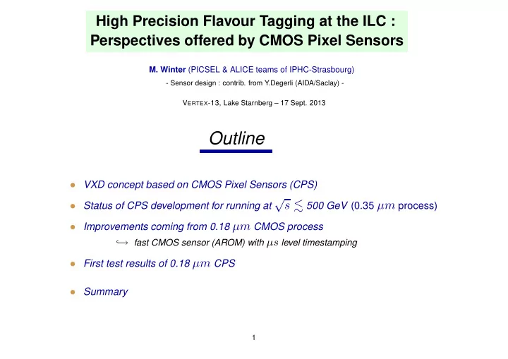
High Precision Flavour Tagging at the ILC : Perspectives offered by CMOS Pixel Sensors M. Winter (PICSEL & ALICE teams of IPHC-Strasbourg) - Sensor design : contrib. from Y.Degerli (AIDA/Saclay) - V ERTEX -13, Lake Starnberg 17 Sept. 2013
High Precision Flavour Tagging at the ILC : Perspectives offered by CMOS Pixel Sensors M. Winter (PICSEL & ALICE teams of IPHC-Strasbourg) - Sensor design : contrib. from Y.Degerli (AIDA/Saclay) - V ERTEX -13, Lake Starnberg – 17 Sept. 2013 Outline • VXD concept based on CMOS Pixel Sensors (CPS) • Status of CPS development for running at √ s � 500 GeV (0.35 µm process) • Improvements coming from 0.18 µm CMOS process → fast CMOS sensor (AROM) with µs level timestamping ֒ • First test results of 0.18 µm CPS • Summary 1
ILC Vertexing Performance Goals • C MOS P IXEL S ENSORS (CPS) devt triggered by ILC vertex detector requirements : � unprecedented granularity & material budget (very low power) � much less demanding running conditions than at LHC ⇛ alleviated read-out speed & radiation tolerance requests � ILC duty cycle ∼ 1/200 ⇛ power saving by power pulsing sub-systems • Vertexing goal: � achieve high efficiency & purity flavour tagging charm & tau !!! → σ Rφ,Z ≤ 5 ⊕ 10 /p · sin 3 / 2 θ µm ֒ ⊲ LHC: σ Rφ ≃ 12 ⊕ 70 /p · sin 3 / 2 θ ⊲ Comparison: σ Rφ,Z (ILD) with VXD made of ATLAS-IBL or ILD-VXD pixels: φ Pointing Z resolution .vs. Pt Pointing R- resolution .vs. Pt 100 100 90 90 m] 80 80 m] µ µ µ µ µ µ µ µ 2 2 2 2 2 2 2 2 µ 3x3 3x3 3x3 3x3 m m m m , 0.15% X , 0.15% X , 0.15% X , 0.15% X 3x3 3x3 3x3 3x3 m m m m , 0.15% X , 0.15% X , 0.15% X , 0.15% X µ resolution [ 0 0 0 0 0 0 0 0 µ µ µ µ µ µ µ µ 2 2 2 2 2 2 2 2 70 14x70 14x70 14x70 14x70 m m m m , 1% X , 1% X , 1% X , 1% X 70 14x70 14x70 14x70 14x70 m m m m , 1% X , 1% X , 1% X , 1% X Pointing Z resolution [ 0 0 0 0 µ µ µ µ 0 0 0 0 µ µ µ µ 2 2 2 2 2 2 2 2 14x70 14x70 14x70 14x70 m m m m , 0.15% X , 0.15% X , 0.15% X , 0.15% X 14x70 14x70 14x70 14x70 m m m m , 0.15% X , 0.15% X , 0.15% X , 0.15% X 0 0 0 0 0 0 0 0 µ µ µ µ µ µ µ µ 2 2 2 2 2 2 2 2 60 3x3 3x3 3x3 3x3 m m m m , 1% X , 1% X , 1% X , 1% X 60 3x3 3x3 3x3 3x3 m m m m , 1% X , 1% X , 1% X , 1% X 0 0 0 0 0 0 0 0 50 50 φ Pointing R- 40 40 30 30 20 20 10 10 0 0 0.91 2 3 4 5 6 7 8 9 10 20 0.91 2 3 4 5 6 7 8 9 10 20 Transverse Momentum [GeV/c] Transverse Momentum [GeV/c] 2
Main Features of CMOS Sensors (CPS) • P-type Si hosting n-type ”charge collectors” • signal created in epitaxial layer (low doping): Q ∼ 70–80 e-h / µm �→ signal � 1000 e − • charge sensing through n-well/p-epi junction • excess carriers diffuse and/or drift to diode with help of reflection on boundaries with p-wells and substrate (high doping) ⇛ continuous signal sensing (no dead time) ⊲ ⊲ ⊲ since a few years : high resistivity ( > 1 k Ω · cm ) epitaxial layer • Prominent advantages of CMOS sensors : granularity : pixels of � 10 × 10 µm 2 ⇛ high spatial resolution (e.g. � 1 µm if needed) ⋄ low material budget : sensitive volume � 10 - 20 µm ⇛ total thickness � 50 µm ⇛ thinning � 50 µm ⋄ signal processing µ circuits integrated in the sensors ⇛ compacity, high data throughput, flexibility, etc. ⋄ industrial mass production ⇛ cost, industrial reliability, fabrication duration, multi-project run frequency, ⋄ technology evolution, ... operating conditions : from ≪ 0 ◦ C to � 30-40 ◦ C ⋄ • Main limitation of the approach : CMOS industry addresses a market far from HEP needs ⋄ fab. process parametres not optimised to fully exploit the potential of CPS ⋄ BUT recently accessible processes (epitaxial layer, feature size) have opened up new perspectives 3
State-of-the-Art: MIMOSA-28 for the STAR-PXL • Details on STAR-PXL in talk of G. Contin 8 May 2013 • Main characteristics of ULTIMATE ( ≡ MIMOSA-28): � rolling shutter read-out derived from EUDET BT chip: MIMOSA-26 � 0.35 µm process with high-resistivity epitaxial layer � column // architecture with in-pixel cDS & amplification � end-of-column discrimination & binary charge encoding � on-chip zero-suppression � active area: 960 colums of 928 pixels (19.9 × 19.2 mm 2 ) � pitch: 20.7 µm ∼ 0.9 million pixels ֒ → charge sharing ⇛ σ sp � 3.5 µm � JTAG programmable � t r.o. � 200 µs ( ∼ 5 × 10 3 frames/s) ⇛ suited to > 10 6 part./cm 2 /s � 2 outputs at 160 MHz � ∼ 150 mW/cm 2 power consumption � N � 15 e − ENC at 30-35 ◦ C � ǫ det versus fake hit rate � Radiation tolerance : 3 · 10 12 n eq /cm 2 & 150 kRad at 30-35 ◦ C � Detector construction under way (40 ladders made of 10 sensors) ⊲⊲⊲ 1st step: Commissioning of 3/10 of detector completed at RHIC with pp collisions in May-June 2013 4
CMOS Pixel Sensors for the ILD-VXD • Two types of CMOS Pixel Sensors : � Inner layers ( � 300 cm 2 ) : priority to read-out speed & spatial resolution → small pixels (16 × 16 / 80 µm 2 ) with binary charge encoding ֒ σ sp � 3 / 6 µm ֒ → t r.o. ∼ 50 / 10 µs ; � Outer layers ( ∼ 3000 cm 2 ) : priority to power consumption and good resolution → large pixels (35 × 35 µm 2 ) with 3-4 bits charge encoding ֒ σ sp � 4 µm ֒ → t r.o. ∼ 100 µs ; � Total VXD instantaneous/average power < 600/12 W (0.18 µm process) • 2-sided ladder concept for inner layer : PLUME coll. � S quare pixels (16 × 16 µm 2 ) on internal ladder face ( σ sp < 3 µm ) & E longated pixels (16 × 64/80 µm 2 ) on external ladder face (t r.o. ∼ 10 µs ) • Final ”500 GeV” CPS prototypes : fab. in Winter 2011/12 ⊲ ⊲ ⊲ � MIMOSA-30: inner layer prototype with 2-sided read-out → one side : 256 pixels (16 × 16 µm 2 ) ֒ other side : 64 pixels (16 × 64 µm 2 ) ⊲ ⊲ ⊲ � MIMOSA-31: outer layer prototype → 48 col. of 64 pixels (35 × 35 µm 2 ) ended with 4-bit ADC ֒ � prototypes were still fabricated in 0.35 µm CMOS process (cost saving) 5
Acceleration of Frame Read-Out • Motivations for faster read-out: � robustness w.r.t. predicted 500 GeV BG rate (keep small inner radius, ...) � standalone inner tracking capability (e.g. soft tracks) � compatibility with high-energy running: expected beam BG at √ s � 1 TeV ≃ 3–5 × BG (500 GeV) • How to accelerate the elongated pixel read-out � elongated pixel dimensions allow for in-pixel discri. ⇛ ≥ 2 faster r.o. � read out simultaneously 2 or 4 rows ⇛ 2-4 faster r.o./side � subdivide pixel area in 4-8 sub-arrays read out in // ⇛ 2-4 faster r.o./side ⊲ 0.18 µm process needed: 6-7 ML, design compactness, in-pixel CMOS T, ... � conservative step: 2 discri./col. end (22 µm wide) ⇛ simult. 2 row r.o. • Expected VXD performances at 1 TeV (and 0.5 TeV) σ sp t int Layer Occupancy [%] Power MIMOSA/AROM MIMOSA/AROM 1 TeV (0.5 TeV) inst./average 3 / 5-6 µm 50 / 2 µs (10 µs ) VXD-1 4.5(0.9) / 0.5(0.1) 250/5 W 4 / 10 µm 100 / 7 µs (100 µs ) VXD-2 1.5(0.3) / 0.2(0.04) 120/2.4 W 4 / 10 µm 100 / 7 µs (100 µs ) VXD-3 0.3(0.06) / 0.05(0.01) 200/4 W 6
Evolving towards an Optimal CMOS Process • Motivation: 0.35 µm process used up to now does not allow to fully exploit the potential of CPS • Main limitations CMOS process In-pixel Read-out Power Insensitive TID Data ( > ILC) of presently used fab. parametres circuitry speed consum. areas throughput 0.35 µm CMOS Feature size X X X X X fabrication process: Planar techno. X X X x Nb (metal layers) X X X (not restricted to Clock frequency X X ILC specs) • Moving to a 0.18 µm imaging CMOS process (Tower/Jazz SC): � Deep P-well (quadruple well techno.) ⇛ small-pitch in-pixel discriminators � 6 metal layers (instead of 4) ⇛ in-pixel discriminators, avoids insensitive zones � Epitaxial layer : thickness ∼ 18–40 µm and resistivity ∼ 1–6 k Ω · cm � Stiching ⇛ multi-chip slabs (yield ?) ⇛ process very well suited to the VXD specifications • Prototyping started in Summer 2011, driven by ILD-VXD, CBM-MVD, ALICE-ITS, etc. 7
Applications of CPS : ALICE-ITS Upgrade • ITS upgrade : scheduled for ”2017-18” LHC long shutdown � see talk of M. Sitta � exploits space left by replacement of beam pipe with small radius (19 mm) section � addition of L0 at ∼ 22 mm radius to present ITS & replacement of (at least) inner part of present ITS � 1st tracker entirely omposed of pixel sensors : ⋄ 7 layers with pixels : � 9 m 2 , O(10 10 ) pixels ! ⋄ material budget of inner layers ∼ 0.3 % X 0 • Differences w.r.t. ULTIMATE/MIMOSA-28 : � ∼ 0.25/1 MRad & 0.3/1 · 10 13 n eq /cm 2 at T = 30 ◦ C (target values) ֒ → 0.18 µm 4-well HR-epi techno. (instead of 0.35 µm 2-well hR-epi) � ∼ 1 × 3 cm 2 large sensitive area (instead of 2 × 2 cm 2 ) � parallelised rolling-shutter (pot. in-pixel discri.) ∼ 10–30 µs � 1 or 2 output pairs at � 300 MHz (instead of 1 output pair at 160 MHz) � σ sp ∼ 4 µm ; ladders ∼ 0.3 % X 0 ⊲⊲⊲ CDR approved by LHCC in Sept. 2012 TDR Draft-1 close to release ⊲⊲⊲ 2 alternative sensors developed at IPHC : MISTRAL (end-of-col discri) & ASTRAL (in-pixel discri) • Extension to CBM-MVD see talk of M. Deveaux 8
CPS fabricated in 0.18 µm Process 9
Recommend
More recommend
Explore More Topics
Stay informed with curated content and fresh updates.
