Outline Introduction and Motivation Performance and Design - PDF document
3D Devices: Experiment & Simulation S. BARRAUD, CEA, LETI, Minatec Campus, Grenoble, FRANCE ESSDERC/ ESSCIRC Workshop Process Variations from Equipment Effects to Circuit and Design Impacts September 3, 2018, Dresden, Germany Slide 1
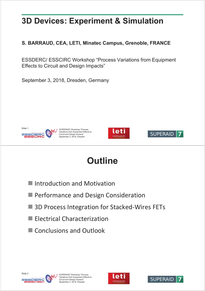
3D Devices: Experiment & Simulation S. BARRAUD, CEA, LETI, Minatec Campus, Grenoble, FRANCE ESSDERC/ ESSCIRC Workshop “Process Variations from Equipment Effects to Circuit and Design Impacts” September 3, 2018, Dresden, Germany Slide 1 SUPERAID7 Workshop “Process Variations from Equipment Effects to Circuit and Design Impacts” September 3, 2018, Dresden Outline � Introduction and Motivation � Performance and Design Consideration � 3D Process Integration for Stacked-Wires FETs � Electrical Characterization � Conclusions and Outlook Slide 2 SUPERAID7 Workshop “Process Variations from Equipment Effects to Circuit and Design Impacts” September 3, 2018, Dresden
Context of this work ? Two main MOSFET architectures for advanced CMOS 14nm SAMSUNG 14nm INTEL 10nm INTEL 3D FinFET 22nm INTEL New MOSFET 16nm TSMC architectures need to be proposed 22nm GF B Back-gate control using 28nm ST thin BOX capacitive th 2D FDSOI Single-gate � reduction Si of of SCE controlled by thinner T Si or T BOX th Slide 3 SUPERAID7 Workshop “Process SUPERAID7 Workshop “Process Variations from Equipment Effects to Circuit and Design Impacts” September 3, 2018, Dresden Context of this work Recent press release May │ 2017 Samsung set to lead the future of foundry with comprehensive process roadmap down to 4nm 4LPP (4nm Low Power Plus): 4LPP will be the first implementation of next generation device architecture – MBCFET TM structure (Multi Bridge Channel FET). MBCFET TM is Samsung’s unique GAAFET ( Gate All Around FET ) technology that uses a Nanosheet device to overcome the physical scaling and performance limitations of the FinFET architecture. https://news.samsung.com/global/samsung-set-to-lead-the-future-of-foundry-with- comprehensive-process-roadmap-down-to-4nm June │ 2017 IBM claims 5nm Nanosheet breakthough IBM researchers and their partners have developed a new transistor architecture based on Stacked Silicon Nanosheets that they believe will make FinFETs obsolete at the 5nm node http://www.eetimes.com/document.asp?doc_id=1331850& GAA MOSFET devices are becoming an industrial reality Slide 4 SUPERAID7 Workshop “Process Variations from Equipment Effects to Circuit and Design Impacts” September 3, 2018, Dresden
Motivation • Wire FETs can be view as an GAA Wire FETs Fin FETs evolutionary step from the FinFET footprint footprint • Wire FETs share many of the same process steps as the FinFET • GAA FETs provides a better electrostatics than FinFET W Fin TCAD results FP FP FinFET W NW =W Fin 60 H fin =45nm W=7nm IMEC [2] 14nm INTEL [1] LETI [3] DIBL (mV/V) L G =10nm 40 GAA 7nm 20 10 15 20 25 30 35 40 [1] S. Natarajan et al. , IEDM, 2014. [2] H. Mertens et al. , VLSI Technology, 2016. Gate length (nm) [3] C. Dupré et al. , IEDM, 2008. Slide 5 SUPERAID7 Workshop “Process Variations from Equipment Effects to Circuit and Design Impacts” September 3, 2018, Dresden Introduction – Goals and Strategy Main Objective of SUPERAID7 Simulation of the impact of systematic and statistical process variations on devices, interconnects and circuits down to the 5nm node WP2: Specifications and benchmarks WP1 Define specifications for two generations of devices ( 7nm Trigate and 5nm Project GAA Stacked-Wires FETs ) – process-flow/morphological data/electrical data… managment → to provide input data for the calibration/validation of simulation tools → to give a feedback to other WP after the comparison between simulation and experiment WP3: Variation- WP4: Variation- aware equipment aware device and and process interconnect simulation simulation WP5: Software integration and compact models Dissemination (WP6) and exploitation (WP7) Slide 6 SUPERAID7 Workshop “Process Variations from Equipment Effects to Circuit and Design Impacts” September 3, 2018, Dresden
Outline � Introduction and Motivation � Performance and Design Consideration � 3D Process Integration for Stacked-Wires FETs � Electrical Characterization � Conclusions and Outlook Slide 7 SUPERAID7 Workshop “Process Variations from Equipment Effects to Circuit and Design Impacts” September 3, 2018, Dresden Performance and Design Consideration Nanowire (NW) FinFET (FF) NW FP=25nm FF Triple Stack (3S) FP=25nm H Fin =43nm H Fin ×3GAA T S =8nm H Fin =43nm H Fin T S H NW =6.3nm W Fin =7nm W NW =7nm S Nanosheet (NS) Nanosheet (NS) NS H Fin H Fin H Fin =43nm T S T S H NS =6.3nm W NS >W NW T S =8nm S Double Stack (1S) ×3GAA Single Stack (2S) ×3GAA Slide 8 SUPERAID7 Workshop “Process Variations from Equipment Effects to Circuit and Design Impacts” September 3, 2018, Dresden
Effective width of FinFET � � �� � � � � �� � � �� � � Footprint ��� �� � �� � � �� � � � � FF FF W=7nm W Fin H Fin =43nm FP 120 Footprint Footprint (nm) 80 W Fin FP 40 Footprint TCAD 0,2 0,4 0,6 0,8 W eff ( μ m) W Fin FP S. Barraud et al., IEDM 2017 Slide 9 SUPERAID7 Workshop “Process Variations from Equipment Effects to Circuit and Design Impacts” September 3, 2018, Dresden FinFET versus GAA Nanowires � � �� � � � � �� � � �� � � ��� �� � �� � � �� � � � � NW NW FF W=7nm FF H Fin =43nm 120 Footprint (nm) -14% ? 80 Improvement of W eff for a constant surface occupation 40 TCAD 0,2 0,4 0,6 0,8 W eff ( μ m) S. Barraud et al., IEDM 2017 Slide 10 SUPERAID7 Workshop “Process Variations from Equipment Effects to Circuit and Design Impacts” September 3, 2018, Dresden
GAA Nanowires versus GAA Nanosheets � � �� � � � � �� � � �� � � +42% W eff ��� �� � �� � � �� � � � � W NS NW 132nm NS 120 Footprint (nm) FF 107nm +24% W eff 82nm 80 57nm 40 × 3GAA 32nm +5% W eff 0,2 0,4 0,6 0,8 +5% W eff ( μ m) Slide 11 SUPERAID7 Workshop “Process Variations from Equipment Effects to Circuit and Design Impacts” September 3, 2018, Dresden Tradeoff between SCE and W eff LF Footprint=57nm Footprint=82nm Footprint=107nm 60 60 60 FF FF FF 50 50 44.5 50 W Fin DIBL (mV/V) FP 82 57 LF 32 NS 24 NS 40 40 40 19.5 NS 15 13 30 30 30 FP W NW =W Fin L G =16nm L G =16nm L G =16nm NW NW NW LF 20 20 20 0,2 0,4 0,4 0,6 0,4 0,6 � ���� ���� � ���� ���� � ���� ���� W NS GAA stacked-nanosheets maximize W eff ( i.e . drive current) per layout footprint with improved channel electrostatics. S. Barraud et al., IEDM 2017 Slide 12 SUPERAID7 Workshop “Process Variations from Equipment Effects to Circuit and Design Impacts” September 3, 2018, Dresden
Power/Performance Optimization FP=25nm; 3 stacked GAA; L G =16nm; H NW =6.5nm LF LF FP=25nm FF 0 10 HP × 3 stacked-wires 44.5nm W Fin FP Normalized I OFF W NS 24nm 57nm 32nm 15nm 19.5nm LF -1 10 13nm LF=57nm FP LP W NW =W Fin LF=82nm LF=107nm W=7nm -2 10 0,5 1,0 1,5 Normalized I ON Slide 13 SUPERAID7 Workshop “Process Variations from Equipment Effects to Circuit and Design Impacts” September 3, 2018, Dresden Parasitic capacitances and delay A delay reduction of around 20% is expected for W NS ~30nm 20 � : Delay LF=82nm (4 fins with FP=25nm) I eff : Effective drive current NW LF=57nm (3 fins with FP=25nm) I eff =(I H +I L )/2 I H =I DS (V GS =V DD , V DS =V DD /2) 10 82nm C eq (%) I L =I DS (V GS =V DD /2, V DS =V DD ) 32nm Supply voltage V DD =0.7V 57nm 15.3nm FO=3 0 19.5nm L G =16nm Spacer size: 4.2nm EOT=0.67nm NW C eq (%) NS � �� � � C back-end =2fF �� (W=7nm) � � -10 M=2: Miller effect in inverter � ����� � � ��� -40 -20 0 20 40 � � � � ��� � � � � � � ��� � �� � � �������� � �� � � � �� �� � � ��� � � � ��� � � p (%) � p (%) Slide 14 SUPERAID7 Workshop “Process Variations from Equipment Effects to Circuit and Design Impacts” September 3, 2018, Dresden
What have we learned? � GAA NS structures could be used to maximize the effective width which will improve the drive current without increasing power density (lower DIBL than in short-channel FinFET devices). � A delay reduction of around 20% is expected for W NS ~30nm � Nanosheet transistors offer more freedom to designers for the power-performance optimization thanks to a fine tuning of the device width Slide 15 SUPERAID7 Workshop “Process Variations from Equipment Effects to Circuit and Design Impacts” September 3, 2018, Dresden Outline � Introduction and Motivation � Performance and Design Consideration � 3D Process Integration for Stacked-Wires FETs � Electrical Characterization � Conclusions and Outlook Slide 16 SUPERAID7 Workshop “Process Variations from Equipment Effects to Circuit and Design Impacts” September 3, 2018, Dresden
Recommend
More recommend
Explore More Topics
Stay informed with curated content and fresh updates.


