Outline Architectures for CMOS EDC Linear equalizer - PDF document
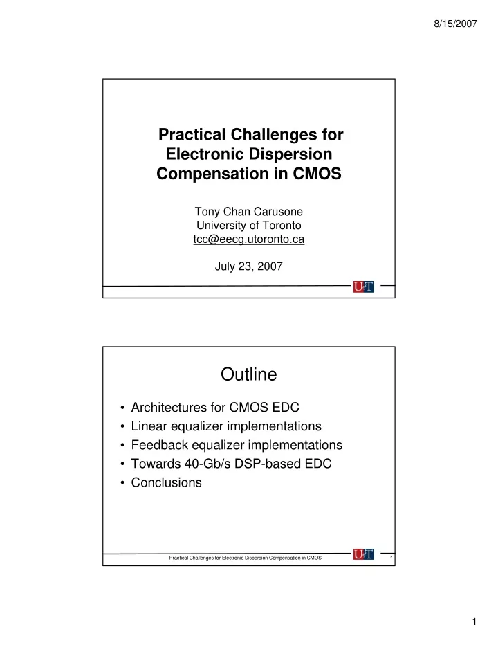
8/15/2007 Practical Challenges for Electronic Dispersion Electronic Dispersion Compensation in CMOS Tony Chan Carusone University of Toronto University of Toronto tcc@eecg.utoronto.ca July 23, 2007 Outline Architectures for CMOS EDC
8/15/2007 Practical Challenges for Electronic Dispersion Electronic Dispersion Compensation in CMOS Tony Chan Carusone University of Toronto University of Toronto tcc@eecg.utoronto.ca July 23, 2007 Outline • Architectures for CMOS EDC • Linear equalizer implementations • Feedback equalizer implementations • Towards 40-Gb/s DSP-based EDC • Conclusions Practical Challenges for Electronic Dispersion Compensation in CMOS 2 1
8/15/2007 Electronic Dispersion Compensation • Perform CD compensation optically • PMD compensation must be adaptive to track changes over milliseconds � Fewer taps than EDC for both CD & PMD EDC Optical CD Comp. Practical Challenges for Electronic Dispersion Compensation in CMOS 3 Electronic Dispersion Compensation • Possibilities –Linear equalization –Decision feedback equalization –MLSE EDC Optical CD Comp. Practical Challenges for Electronic Dispersion Compensation in CMOS 4 2
8/15/2007 DFE Design Parameters CLK IN IN OUT OUT b 0 τ F τ B b 1 a 1 τ F τ B b 2 a 2 2 2 Practical Challenges for Electronic Dispersion Compensation in CMOS 5 DFE Design Parameters CLK IN IN OUT OUT b 0 τ F τ B b 1 a 1 τ F τ B b 2 a 2 2 2 Feedback Linear Equalizer Equalizer Practical Challenges for Electronic Dispersion Compensation in CMOS 6 3
8/15/2007 DFE Design Parameters CLK IN IN OUT OUT b 0 τ F τ B b 1 a 1 τ F τ B b 2 a 2 2 2 Challenges: • Extendibility of analog/mixed- • Inherent delay-bandwidth-gain signal approaches to long tradeoffs impulse responses • Timing critical path in the feedback equalizer Practical Challenges for Electronic Dispersion Compensation in CMOS 7 DFE Design Parameters CLK IN IN OUT OUT b 0 } { τ F τ B b 1 a 1 N B N F τ F τ B b 2 a 2 2 2 • N F and N B are chosen just large enough to cover the worst-case (i.e. longest) fiber pulse response Practical Challenges for Electronic Dispersion Compensation in CMOS 8 4
8/15/2007 DFE Design Parameters CLK IN IN OUT OUT b 0 } { τ F τ B b 1 a 1 N B N F τ F τ B b 2 a 2 2 2 • τ B is generally equal to one bit period since OUT is updated by the clock Practical Challenges for Electronic Dispersion Compensation in CMOS 9 DFE Design Parameters CLK IN IN OUT OUT b 0 } { τ F τ B b 1 a 1 N B N F τ F τ B b 2 a 2 2 2 • τ F can either be one bit period or a fraction thereof Practical Challenges for Electronic Dispersion Compensation in CMOS 10 5
8/15/2007 Fractional vs. Baud-Rate Tap-Spacing 4 • Fractional tap-spacing introduces 3 correlation between neighboring ing tap signals p g ate 2 Tap Weights s Baud-Ra � This can cause the adaptation Tap-Spac 1 engine to become “confused” and 0 to converge slowly, or diverge -1 • Example: – 7-tap linear equalizer -2 – Ideal LMS adaptation -3 0 2000 4000 6000 8000 10000 Time [UI] 4 0.5 aud /2 3 0.4 g 2 2 Fractional T ba Tap-Spacin Pulse Response Tap Weights 0.3 1 0.2 0 -1 0.1 -2 0 0 2 4 6 8 Time [UI] -3 0 2000 4000 6000 8000 10000 Time [UI] Practical Challenges for Electronic Dispersion Compensation in CMOS 11 Fractional vs. Baud-Rate Tap-Spacing Baud-Rate Fractional Tap-Spacing T S i Tap-Spacing T S i 2 2 1 1 Eye Pattern Eye Pattern 0 0 -1 -1 -2 -2 0 0.5 1 1.5 2 0 0.5 1 1.5 2 Time [UI] Time [UI] � Negligible difference in performance Practical Challenges for Electronic Dispersion Compensation in CMOS 12 6
8/15/2007 Implementation of Linear Equalizer Feedback Equalizer Decision Linear VGA Equalizer Circuit Practical Challenges for Electronic Dispersion Compensation in CMOS 13 3-Tap Traveling Wave Filter Passive delay lines consume no power Practical Challenges for Electronic Dispersion Compensation in CMOS 14 7
8/15/2007 3-Tap Traveling Wave Filter Practical Challenges for Electronic Dispersion Compensation in CMOS 15 3-Tap Traveling Wave Filter Practical Challenges for Electronic Dispersion Compensation in CMOS 16 8
8/15/2007 3-Tap Traveling Wave Filter τ = Tap spacing : 2 LC 1 2 = = Delay Line Bandwidth : f πτ 3dB π LC ∝ Maximum gain per tap C Practical Challenges for Electronic Dispersion Compensation in CMOS 17 3-Tap Traveling Wave Filter • Example: Simulated 3-section lumped-LC delay line designed for 25-ps tap spacing (baud-rate line designed for 25 ps tap spacing (baud rate tap spacing at 40 Gb/s) Practical Challenges for Electronic Dispersion Compensation in CMOS 18 9
8/15/2007 6-Tap Traveling Wave Filter τ = Tap spacing : LC 2 2 = = Delay Line Bandwidth : f πτ 3dB π LC ∝ Maximum gain per tap C / 2 Practical Challenges for Electronic Dispersion Compensation in CMOS 19 6-Tap Traveling Wave Filter • Example: Simulated 6-section lumped-LC delay line designed for the same total delay line designed for the same total delay Practical Challenges for Electronic Dispersion Compensation in CMOS 20 10
8/15/2007 3-Tap Crossover TWF Practical Challenges for Electronic Dispersion Compensation in CMOS 21 3-Tap Crossover TWF Practical Challenges for Electronic Dispersion Compensation in CMOS 22 11
8/15/2007 3-Tap Crossover TWF Practical Challenges for Electronic Dispersion Compensation in CMOS 23 3-Tap Crossover TWF Practical Challenges for Electronic Dispersion Compensation in CMOS 24 12
8/15/2007 3-Tap Crossover TWF τ = Tap spacing : 2 LC 2 4 = = Delay Line Bandwidth : f πτ 3dB π LC ∝ Maximum gain per tap C Practical Challenges for Electronic Dispersion Compensation in CMOS 25 Summary Tap Delay line Max. gain spacing i b bandwidth d idth per tap t 1 ∝ C 3-tap TWF 2 LC π LC 2 ∝ C / 2 6-tap TWF p LC LC π LC 2 ∝ 2 LC C 3-tap CTWF π LC Practical Challenges for Electronic Dispersion Compensation in CMOS 26 13
8/15/2007 Prototype Implementation • 90-nm CMOS process • 24 mW from 1-V supply Practical Challenges for Electronic Dispersion Compensation in CMOS 27 30-Gb/s Equalizer in 90-nm CMOS Jonathan Sewter, M.A.Sc. 500 μ m 600 μ m Practical Challenges for Electronic Dispersion Compensation in CMOS 28 14
8/15/2007 30-Gb/s Equalizer in 90-nm CMOS Jonathan Sewter, M.A.Sc. Output Output T-line Digital Controls Gain Cells 500 μ m Input T-line p Preamplifier Input 600 μ m Practical Challenges for Electronic Dispersion Compensation in CMOS 29 Input and output eye diagrams at 20 Gb/s over 12-dB loss channel Practical Challenges for Electronic Dispersion Compensation in CMOS 30 15
8/15/2007 Input and output eye diagrams at 25 Gb/s over 13-dB loss channel Practical Challenges for Electronic Dispersion Compensation in CMOS 31 Input and output eye diagrams at 30 Gb/s over 14-dB loss channel Practical Challenges for Electronic Dispersion Compensation in CMOS 32 16
8/15/2007 3-Tap Crossover TWF τ = Tap spacing : 2 LC 2 4 = = Delay Line Bandwidth : f πτ 3dB π LC ∝ Maximum gain per tap C Practical Challenges for Electronic Dispersion Compensation in CMOS 33 3-Tap Crossover TWF τ = Tap spacing : 2 LC 3 6 = = Delay Line Bandwidth : f ??? πτ 3dB π LC ∝ Maximum gain per tap C Practical Challenges for Electronic Dispersion Compensation in CMOS 34 17
8/15/2007 3-Tap Crossover TWF Practical Challenges for Electronic Dispersion Compensation in CMOS 35 3-Tap Crossover TWF • Problem: The crossover routing could introduce skew and crosstalk between paths that must be matched Practical Challenges for Electronic Dispersion Compensation in CMOS 36 18
8/15/2007 Folded-Cascade TWF • Solution: Alleviate Solution: Alleviate crossover routing by introducing an intermediate “folded” transmission line Practical Challenges for Electronic Dispersion Compensation in CMOS 37 Folded-Cascade TWF • Each path through this network goes through network goes through 5 delay sections and 2 amplifiers Practical Challenges for Electronic Dispersion Compensation in CMOS 38 19
8/15/2007 Folded-Cascade TWF • Each path through this network goes through network goes through 5 delay sections and 2 amplifiers • Each path has a gain of a 2 (assuming lossless delay y elements) Practical Challenges for Electronic Dispersion Compensation in CMOS 39 Folded-Cascade TWF • Each path through this network goes through g g 5 delay sections and 2 amplifiers • Each path has a gain of a 2 (assuming lossless delay elements) elements) • There are 9 such paths � Total gain through this tap is 9 a 2 Practical Challenges for Electronic Dispersion Compensation in CMOS 40 20
8/15/2007 Folded-Cascade TWF Distributed Amp. #2 • Alternate interpretation: interpretation: This is a cascade of 2 distributed amplifiers • Each has a gain of 3 a (assuming 3 a (assuming lossless delay elements) Distributed Amp. #1 � Total gain is 9 a 2 Practical Challenges for Electronic Dispersion Compensation in CMOS 41 3-Tap Folded-Cascade TWF Tap 1 Tap 1 Tap 2 Tap 2 Tap 3 Tap 3 • Example: 3-tap FIR filter Practical Challenges for Electronic Dispersion Compensation in CMOS 42 21
Recommend
More recommend
Explore More Topics
Stay informed with curated content and fresh updates.
