Outcomes I know the difference between combinational and sequential - PowerPoint PPT Presentation
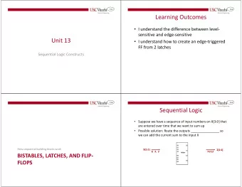
1-6.1 1-6.2 Outcomes I know the difference between combinational and sequential logic and can name examples of each. I understand latency, throughput, and at least 1 technique to Spiral 1 / Unit 6 improve throughput I can identify
1-6.1 1-6.2 Outcomes • I know the difference between combinational and sequential logic and can name examples of each. • I understand latency, throughput, and at least 1 technique to Spiral 1 / Unit 6 improve throughput • I can identify when I need state vs. a purely combinational Flip-flops and Registers function – I can convert a simple word problem to a logic function (TT or canonical form) or state diagram • I can use Karnaugh maps to synthesize combinational functions with several outputs • I understand how a register with an enable functions & is built • I can design a working state machine given a state diagram • I can implement small logic functions with complex CMOS gates 1-6.3 1-6.4 Flip-Flops • Outputs only change once per clock period – Outputs change on either the positive edges of the clock or the negative edges FLIP FLOPS AND REGISTERS Positive-Edge of the Clock Negative-Edge of the Clock
1-6.5 1-6.6 Flip-Flops Positive-Edge Triggered D-FF • To indicate negative-edge triggered use a bubble in • Q looks at D only at CLK D Q* Q’* front of the clock input the positive-edge 0 x Q Q ’ 1 x Q Q ’ ↑ 0 0 1 ↑ Positive-Edge Triggered Negative-Edge Triggered 1 1 0 D-FF D-FF D Q D Q CLK D-FF D-FF Q Q D CLK CLK Q No bubble indicates Bubble indicates positive-edge negative-edge Q only samples D at the positive edges and then triggered triggered holds that value until the next edge 1-6.7 1-6.8 Negative-Edge Triggered D-FF D FF Example • Q looks at D only at • Assume positive edge-triggered FF CLK D Q* Q’* the negative-edge 0 x Q Q ’ 1 x Q Q ’ ↓ 0 0 1 ↓ 1 1 0 CLK D Q Q only samples D at the negative edges and then holds that value until the next edge
1-6.9 1-6.10 D FF Example Shift Register • Assume negative edge-triggered FF • A shift register is a device that acts as a ‘queue’ or ‘FIFO’ (First-in, First-Out). • It can store n bits and each bit moves one step forward each clock cycle – One bit comes in the overall input per clock – One bit ‘falls out’ the output per clock 1-6.11 1-6.12 Shift Register INITIALIZING OUTPUTS
1-6.13 1-6.14 Initializing Outputs Initializing Outputs • Need to be able to initialize Q to a known value (0 or 1) • To help us initialize our FF’s use a RESET signal • FF inputs are often connected to logic that will produce values – Generally produced for us and given along with CLK after initialization • It starts at Active (1) when power turns on and then • Two extra inputs are often included: PRESET and CLEAR goes to Inactive (0) for the rest of time • When it’s active use it to initialize the FF’s and then it will go inactive for the rest of time and the FF’s will When CLEAR = active SET work based on their inputs Q*=____ Logic D Q When SET = active Q*=____ CLK When NEITHER = active CLR Normal FF operation Inactive (0) for the rest of time RESET Active (1) at time=0 Note: SET and CLR have priority over normal FF inputs 1-6.15 1-6.16 Initializing Outputs Implementing an Initial State • Need to be able to initialize Q to a known value (0 or 1) • When RESET is activated Q’s initialize to 0 and then when it goes back to 1 the Q’s look at the D inputs When RESET = 0, Forces Q’s to 0 because it’s CLR is inactive and RESET connected to the CLR inputs Q looks at D at each clock edge RESET 0 0 Once RESET goes to 0, the FF’s SET Q* = _ Q0 look at the D inputs SET Q* = _ ... D Q Logic Logic D Q CLK CLK Q1 ... CLR CLR RESET RESET 1 0
1-6.17 1-6.18 Preset / Clear Example • Assume an synchronous Preset 1 3 5 7 D CLK Using muxes to control when register save data CLR REGISTER WITH ENABLES SET Q 1-6.19 1-6.20 Register Resets/Clears Register Problem • Whatever the D value is at the clock edge is sampled D0 Q0 D Q • When the power turns on the bit CLR and passed to the Q output until the next clock edge stored in a flip-flop will initialize to a ____________ value • Problem: Register will save data on ________ edge D1 D Q Q1 • Better to initialize it to a known – Often we want the ability to save on one edge and then CLR value (____________) ___________ that value for many more cycles • Use a special signal called "______" D Q Q2 D2 to force the flip-flops to 0's CLR CLK RST CLK RST D i Q i * D3 D Q Q3 D[3:0] 0010 0011 0100 0101 0110 0111 1000 1001 1010 CLR 1,0 X X Q i Q[3:0] ? 0000 0011 0100 0101 0110 0111 1000 1001 ↑ RST ↑ CLK 4-bit Register – On clock edge, D is passed to Q ↑ 4-bit Register
1-6.21 1-6.22 Solution Registers w/ Enables Q • Registers (D-FF’s) will sample the D • When EN=0, Q value is 0 Q bit every clock edge and pass it to Q 0 D Q Q Y Q Y D Q D 1 passed back to the input S • Sometimes we may want to hold the 1 D S CLR 0 EN CLR value of Q and ignore D even at a and thus Q will maintain its CLK EN RST clock edge CLK value at the next clock edge RST • We can add an enable input and When EN=0, Q is some logic in front of the D-FF to FF with Data Enable • When EN=1, D value is recycled back to the input accomplish this (Always clocks, but selectively passed to the input and chooses old value, Q, or new value D) thus Q will change at the CLK RST EN D i Q i * 0 D Q edge based on D Y D Q D 0,1 X X X Q i D 1 S CLR 1 ↑ 1 X X 0 EN CLK ↑ RST ↑ When EN=1, D input is ↑ passed to FF input 1-6.23 1-6.24 Registers w/ Enables 4-bit Register w/ Data (Load) Enable 0 Y D Q Q0 • Registers (D-FF’s) will sample the D • The D value is sampled at the clock edge only D0 1 S CLR bit every clock edge and pass it to Q if the enable is active • Sometimes we may want to hold the 0 Y D Q Q1 value of Q and ignore D even at a 1 D1 S • Otherwise the current Q value is maintained CLR clock edge • We can add an enable input and 0 some logic in front of the D-FF to Y D Q Q2 1 D2 S accomplish this CLR CLK 0 Y D Q Q3 CLK RST EN D i Q i * 1 RST D3 S CLR 0,1 X X X Q i EN EN RST ↑ 1 X X 0 CLK D[3:0] 0010 0011 0100 0101 0110 0111 1000 1001 1010 ↑ 0 0 X Q i 4-bit register with 4-bit wide 2-to-1 mux in front Q[3:0] 0000 0101 0111 1000 ↑ 0 1 0 0 of the D inputs ↑ 0 1 1 1
Recommend
More recommend
Explore More Topics
Stay informed with curated content and fresh updates.


