Melt infiltrated/textured YBCO bulks with artificially patterned - PowerPoint PPT Presentation
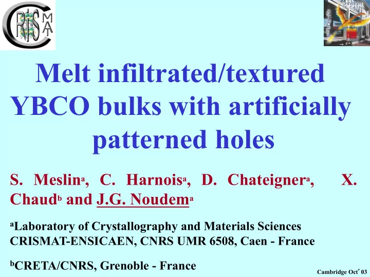
Melt infiltrated/textured YBCO bulks with artificially patterned holes S. Meslin a , C. Harnois a , D. Chateigner a , X. Chaud b and J.G. Noudem a a Laboratory of Crystallography and Materials Sciences CRISMAT-ENSICAEN, CNRS UMR 6508, Caen -
Melt infiltrated/textured YBCO bulks with artificially patterned holes S. Meslin a , C. Harnois a , D. Chateigner a , X. Chaud b and J.G. Noudem a a Laboratory of Crystallography and Materials Sciences CRISMAT-ENSICAEN, CNRS UMR 6508, Caen - France b CRETA/CNRS, Grenoble - France Cambridge Oct ’ 03
Aim •facilitate the sample oxygenation and decrease the crack number in the ab planes •decrease the number of voids and pores in large samples •simplify the sample shaping for fault current limiters •improve the sample cooling during applications, avoiding hot spots Cambridge Oct ’ 03
State of the art • Preparation of regular arrays of antidots in Y123 thin films and observation of vortex lattice matching effets A. Castellanos, P. Selders, M. Vaupel, R. Wördenweber, G. Ockenfuss, A. v.d. Hart and K. Keck : EUCAS (1997) the Netherlands •Superconducting foam R.E. Suddakar and G.J. Schmitz SST 15(2002) L21 • Growth of single domains through sintered YBaCuO pellets drilled with an array of holes for the fabrication of c-axis superconducting elements for current limitation application R. Tournier, X. Chaud, D. Isfort, L. Porcar, G. Kapelski : Pasreg-2003 Jena (Germany ) Cambridge Oct ’ 03
Samples preparation Composition : TSMG : Y123 + Y211 (25 mol %) + CeO 2 +SnO 2 IG : (Y035+x%Y123) / Y211+ CeO 2 +SnO 2 Process : •sintering (920°C - 12 hours) •drilling (0.5 to 2 mm diameter holes) •conventionnal TSMG and/or melt infiltration growth (Sm123 seed) Cambridge Oct ’ 03
As-process samples c-axis Cambridge Oct ’ 03
Microstructures Seed location Cambridge Oct ’ 03
Meander shape/fault current limiter elements c-axis c-axis Cambridge Oct ’ 03
{006} Pole figure Cambridge Oct ’ 03
Field mapping : FC (0.4 T, 77K) With hole Without hole 1.00E+00 1.00E+00 7.50E-01 7.50E-01 Normalised trapped field 5.00E-01 trapped field Normalised 5.00E-01 2.50E-01 2.50E-01 X (Step=0.2 mm) X (Step=0.2 mm) 0.00E+00 0.00E+00 Y ( S t e p = 0 . 2 m Y (Step=0.2 mm) m ) Similar values of the trapped field No significant perturbation induced by the holes Cambridge Oct ’ 03
Critical current density Cambridge Oct ’ 03
Conclusion and outlook The perforated samples exhibit a c-axis grain orientation confirmed by pole figure and the single domain character is evidenced by trapped-field distribution. SEM studies have shown that the hole presence does not hinder the domain growth and that the typical microstructure is conserved. Further investigations concerning oxygenation effect, transport-J c measurements, maximum trapped field capacity and interconnected of regular holes are under way. Cambridge Oct ’ 03
Recommend
More recommend
Explore More Topics
Stay informed with curated content and fresh updates.
