ARTIFICIALLY LAYERED FERROELECTRIC OXIDES AND THEIR USES IN THE - PowerPoint PPT Presentation
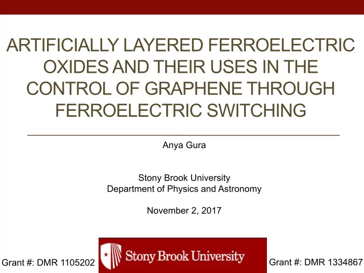
ARTIFICIALLY LAYERED FERROELECTRIC OXIDES AND THEIR USES IN THE CONTROL OF GRAPHENE THROUGH FERROELECTRIC SWITCHING Anya Gura Stony Brook University Department of Physics and Astronomy November 2, 2017 Grant #: DMR 1334867 Grant #: DMR
ARTIFICIALLY LAYERED FERROELECTRIC OXIDES AND THEIR USES IN THE CONTROL OF GRAPHENE THROUGH FERROELECTRIC SWITCHING Anya Gura Stony Brook University Department of Physics and Astronomy November 2, 2017 Grant #: DMR 1334867 Grant #: DMR 1105202
Outline Introduction to perovskite oxides, ferroelectrics, and superlattices • Growth, fabrication, and measurement techniques • PbTiO 3 /SrTiO 3 superlattice system; 2DEG and photocurrent • Surface morphology of SrRuO 3 during growth • Graphene/Ferroelectric hybrid devices •
• Introduction to perovskite oxides, ferroelectrics, and superlattices
What are ferroelectrics? u Insulating materials with two or more discrete states of nonzero electric polarization (spontaneous polarization) in zero applied electric field which switches once an electric field is turned on. u Ferroelectrics are both piezoelectic and pyroelectric, making them useful in many device applications such as • non-volatile memory • thermal detectors • piezoelectric applicators
Perovskite oxides Low temperature distortions High temperature phase oxygen rotation ferroelectricity ABO 3 Perovskite Structure - A-site driven - B-site driven - Also known as antiferrodistortion - Out-of-plane (AFD) A atoms B atom (corners) (Ti) Oxygen atoms Ex: SrTiO 3 Ex: BaTiO 3
Double well potential Landau- Ginzberg- Devonshire approximation Model ferroelectric energy landscape. The double well is the characteristic feature of ferroelectrics. Ferroelectric phase
Polarization switching • Signature property of ferroelectrics is the switchability of polarization • Evidence of switching polarization can be seen in the P-E hysteresis loop (also the effect of E field on double well) Coercive field • The polarization displays hysteric behavior- producing the so-called ‘P-E hysteresis loop’ that is characteristic of ferroelectrics.
Domain switching Polarization reversal is not an instantaneous process. It is preceded by (i) Domain nucleation (ii) Forward Growth (iii) Sideways Growth (Ref: ‘Physics of thin-film ferroelectric oxides ’, Reviews of Modern Physics Vol. 77, No. 4, M. Dawber et al. (2005))
Domains Perfect screening + + + + + + + + + + + + + Polarization over the entire - - - - - - - - - - - - - - crystal is typically not uniform. Regions of uniform polarization P (domains) form with different + + + + + + + + + + + + + - - - - - - - - - - - - - - - - - - - - - - - - - - - - orientations to one another. E D P + + + + + + + + + + + + + - - - + + + - - - + + + P + + + - - - + + + - - - -Bound charges arise at the surface of a polarized dielectric material causing a depolarizing field, E D , which is energetically costly -To compensate, a polydomain configuration of periodic domains Domain walls for 180◦ domains with altering polarization forms. (stripe domains) in a tetragonal perovskite ferroelectric. - As a result, the bound surface charge vanishes on average and the magnitude of the local depolarizing fields is greatly reduced.
Ferroelectric superlattices Interesting properties arise in a superlattice system for many reasons, including size and strain effects in the individual layers, competition between the properties of the constituent materials, and interactions at the interfaces. Bilayer The thickness of a bilayer is called the bilayer wavelength (Λ) A ferroelectric superlattice is a structure created by repeatedly stacking ultrathin layers of materials on top of a substrate, all of which have a similar crystal structure, allowing coherent epitaxial growth. Novel material systems can be engineered by altering the composition and/or thickness of the layers, allowing for the tuning of the material properties.
• Growth, fabrication, and measurement techniques
Growth Sputter deposition: • A type of physical vapor deposition • Uses Ar ions in order to eject particles from a target of the desired material Off-axis RF Magnetron Sputter Deposition Chamber at Stony Brook The sputtering chamber is The sputter system in our electrically grounded and lab is a custom designed therefore acts as an anode vacuum chamber that with the gun as a cathode, allows for up to 6 different and so the electric field is materials to be grown then much higher near the without breaking vacuum. sputter gun, which causes the Ar ions to accelerate towards the target.
X-ray Diffraction X-ray diffraction (XRD) methods are used to study the crystal Reciprocal Space Map structure of these superlattice systems to find properties such as (113) of PTO/SRO • lattice parameters • crystal quality • film thickness • evidence of ferroelectric domains. Λ is the new periodicity of the The diffraction pattern resulting system, so Bragg’s condition changes from the periodic structure of to: the ions in a crystal can be expressed as Bragg’s law: The peaks resulting from the 2 θ - ω Incident beam Diffracted beam scan can be used to find characteristics about the superlattice. Reciprocal space maps can be used to determine: • if a sample has coherently grown on a substrate • determine lattice parameters • examine samples for the presence of ferroelectric domains.
Atomic Force Microscopy (AFM) The topography mode of the AFM can show the surface roughness of the substrate and sample. Other AFM techniques I use include Piezoforce Microscopy and Contact Mode Force Microscopy.
Device Fabrication UV light or e-beam Resist Resist Exposure Development Etching Metalizing Lift-off preparation e-beam Evaporation lithography system deposition chamber for metallization Plasma etcher
• PTO/STO superlattice system; 2DEG and photocurrent
PTO/STO superlattice system STO PTO 100nm STO thick PTO STO PTO SRO bottom electrode STO substrate Two coupling regimes: • Strong coupling (STO layer < 3 u.c.); polarization continuous layer-to-layer • Weak coupling (STO layer > 3 u.c.); layers are decoupled and PTO layers act like thin films (https://wikiar2011.bsc.es/index.php5/Strain_tunning_of_ferroelectric-antiferrodistortive_coupling_in_PbTiO3/SrTiO3_superlattices’, Barcelona Supercomputing Center)
Domain sizes in (n/3) PTO/STO superlattices So far we know that for (n/3) PTO/STO superlattices: • Polarization is continuous throughout the layers • Compressive strain on PTO causes out-of plane 180° domain structure But how does the domain size scale with PTO layer thickness? Competition of screening mechanisms? Kittel power law for ferroelectrics: to minimize the total energy in ferroelectric thin films, a stripe domain configuration forms where the domain width is proportional to the square root of the film thickness
2DEGs at oxide interfaces Theorists use Landau model to investigate whether a monodomain Above a critical thickness of lanthanum aluminate state can be stabilized at PTO/STO interface by means of electronic (LAO) there is a formation of 2D electron gas at the reconstruction. Confirm that ferroelectricity can be used to induce heterointerface of LAO/STO which makes the the formation of 2DEGs at the interface with nonpolar substrates. interface superconducting. The polar discontinuity is energetically costly and to Investigating the relative stability of the two phases by comparing compensate, electrons accumulate at the interface to the thickness evolution of the energy, they arrive at the conclusion screen the discontinuity via electronic that ferroelectric monodomain polarization can exist reconstruction. (Ref: ‘A high-mobility electron gas at the LaAlO3/SrTiO3 heterointerface.’, Ohtomo, (Ref: ‘Model of two-dimensional electron gas formation at ferroelectric interfaces’, Aguado- A., and H. Y. Hwang, Nature 427.6973 (2004): 423-426.’‘Microlithography of electron Puente et al., Phys. Rev. B 92, 035438 (2015) and ‘Two dimensional electron gas at the gases formed at interfaces in oxide heterosctructures’, C. W. Schneiderat al., APL PTO/STO interface: An ab initio study, Binglun Yin et al., Phys. Rev. B 92,115406 (2015)) 89, 122101 (2006))
Probing the PTO/STO interface Metalize Grow superlattice Etch some of it away STO PTO STO Pd Pd PTO STO PTO STO substrate STO substrate STO substrate
Photocurrent in PTO/STO
• Evolution of the surface morphology of SrRuO 3 during growth
̇ ̇ SrRuO 3 surface: a key step in heterostructure synthesis 4 A -0.5 Height -1.0 Typical SrTiO 3 surface -1.5 -2.0nm 0.0 0.5 1.0 1.5 µm 5 -1 8 A 4 -2 Height -3 SrRuO 3 3 -4 SrTiO 3 -5nm 2 0.0 0.5 1.0 1.5 2.0 2.5 µm 1 5 2.0nm 0 2nm 4 0 1 2 3 4 5 Height 1.0 µm 3 0.0 2 0 100 200 300 400 500 1 nm 0 0 1 2 3 4 5 µm GOAL: Systematic study of SrRuO 3 film morphology to control the growth regime and step bunching
Recommend
More recommend
Explore More Topics
Stay informed with curated content and fresh updates.
