Main Memory Moving further away from the CPU .. 95 Main Memory - PDF document
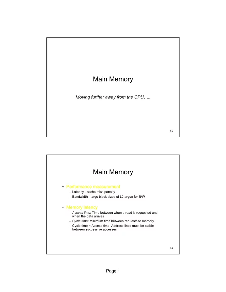
Main Memory Moving further away from the CPU .. 95 Main Memory Performance measurement Latency - cache miss penalty Bandwidth - large block sizes of L2 argue for B/W Memory latency Access time : Time between when a read is
Main Memory Moving further away from the CPU … .. 95 Main Memory • Performance measurement – Latency - cache miss penalty – Bandwidth - large block sizes of L2 argue for B/W • Memory latency – Access time : Time between when a read is requested and when the data arrives – Cycle time : Minimum time between requests to memory – Cycle time > Access time: Address lines must be stable between successive accesses 96 Page 1
Main Memory DIMM controller channel m m m m CPU MC m m m m cache miss request to memory send address, command, data wait for memory to return 97 Hierarchical Organization System 1. Channel – independent connection to DIMMs 2. DIMM – independent modules of memory chips 3. Rank – independent set of chips on each DIMM 4. Chip – individual memory chip of Rank/DIMM 5. Bank – internal independent memory partition 6. Row – internally cached row of a bank Internal 98 Page 2
DIMM organization Rank 0 Rank 1 • Dual Inline Memory Module – Two-sided group of memory chips – Connected to channel – Receives addresses, commands, data side view – Each side is rank of multiple (4,8) chips Chip (8) DIMM front view Pins 99 Rank organization • Independent group of chips on front/back • Connected to the channel Rank 0 Rank 1 cmd/addr select data (64b) from/to channel connection 100 Page 3
Rank organization • Multiple memory chips per rank • Each chip provides part of data • Data size is typically 64 bits chip 0 chip 1 chip 2 chip 3 chip 4 chip 5 chip 6 chip 7 0-7 8-15 56-63 64 bit word (multiple words delivered) 101 Bank • Internal to each chip • Partition of bits accessed independently n banks (4/8) Bank 0 Internal to each chip. Banks receive commands, and operate independently 102 Page 4
Bank e.g. 2kb 2D array 1 bit e.g. 16k Row buffer … Column mux 103 Bank 1 1 0 1 1 0 1 0 1 1 1 1 0 1 1 0 0 1 0 1 0 1 0 1 0 1 1 0 1 1 0 1 Access 0 1 0 1 1 1 0 1 Read Row 3 0 0 0 1 0 0 1 1 Col 5 1 0 1 1 0 1 1 0 1 1 1 1 0 0 1 0 … 104 Page 5
Bank 0 1 1 0 1 1 0 1 Access Read Row 3 Col 5 … Activate Row 105 Bank 0 1 1 0 1 1 0 1 Access Read Row 3 Col 5 0 1 1 0 1 1 0 1 … Sense Row 106 Page 6
Bank Access Read Row 3 Col 5 0 1 1 0 1 1 0 1 … Deliver Data 107 Bank Access Read Row 3 Col 5 0 1 1 0 1 1 0 1 … Rewrite Row 108 Page 7
Bank 0 1 1 0 1 1 0 1 Access Read Row 3 Col 5 … Prepare for next 109 Bank 1 1 0 1 1 0 1 0 1 1 1 1 0 1 1 0 0 1 0 1 0 1 0 1 0 1 1 0 1 1 0 1 0 1 0 1 1 1 0 1 0 0 0 1 0 0 1 1 1 0 1 1 0 1 1 0 1 1 1 1 0 0 1 0 … 110 Page 8
Bit Cell • Structure used to store logical 0 or 1 • Stored as a charge Word line Applications Note Understanding DRAM Operation Overview Figure 1: IBM Trench Capacitor Memory Cell Dynamic Random Access Memory (DRAM) devices are used in a wide range of electronics applications. Although they are produced in many sizes and sold Row Address in a variety of packages, their overall operation is Column Address Word Line Transfer Node Bit Line Strap essentially the same. P+ P+ DRAMs are designed for the sole purpose of storing data. The only valid operations on a memory device N-well are reading the data stored in the device, writing (or P- Substrate Pass transistor storing) data in the device, and refreshing the data periodically. To improve efficiency and speed, a number of methods for reading and writing the mem- Trench Capacitor ory have been developed. This document describes basic asynchronous Note: Not to Scale DRAM operation, including some of the most com- monly used features for improving DRAM perfor- mance. While many aspects of a synchronous DRAM are similar to an asynchronous DRAM, syn- Support Circuitry chronous operation differs because it uses a clocked interface and multiple bank architecture. Additional The memory chip's support circuitry allows the user information regarding specific features and design to read the data stored in the memory's cells, write to issues may be found in the Applications Notes. the memory cells, and refresh memory cells. This circuitry generally includes: DRAM Architecture • Sense amplifiers to amplify the signal or charge detected on a memory cell. DRAM chips are large, rectangular arrays of mem- ory cells with support logic that is used for reading • Address logic to select rows and columns. and writing data in the arrays, and refresh circuitry to maintain the integrity of stored data. • Row Address Select (RAS) and Column Address Select (CAS) logic to latch and resolve the row and column addresses and to initiate Memory Arrays Capacitor and terminate read and write operations. Memory arrays are arranged in rows and columns of • Read and write circuitry to store information in memory cells called wordlines and bitlines, respec- the memory's cells or read that which is stored tively. Each memory cell has a unique location or there. address defined by the intersection of a row and a • Internal counters or registers to keep track of the column. refresh sequence, or to initiate refresh cycles as needed. Memory Cells • Output Enable logic to prevent data from appearing at the outputs unless specifically A DRAM memory cell is a capacitor that is charged to produce a 1 or a 0. Over the years, several differ- desired. Bit line ent structures have been used to create the memory cells on a chip. In today's technologies, trenches filled with dielectric material are used to create the capacitive storage element of the memory cell. 12/96 Page 1 1 transistor (access) + 1 capacitor (storage) physical implementation (from IBM) 111 Bit Cell • Structure used to store logical 0 or 1 • Stored as a charge WRITE bit cell Word line 1. Load value into row buffer 2. Enable word line Pass transistor 3. If 1, capacitor is charged 4. If 0, capacitor is discharged Capacitor Bit line 1 transistor (access) + 1 capacitor (storage) 112 Page 9
Bit Cell • Structure used to store logical 0 or 1 • Stored as a charge READ bit cell Word line 1. Bit line charged 1/2 2. Enable word line Pass transistor 3. Value in cap read onto bit line 4. Bit line swings high/low 5. Sense amp detects swing Capacitor 6. Value is “latched” in row buffer 7. Restore row Bit line Sense amp part of row buffer 1 transistor (access) + 1 capacitor (storage) Read is destructive 113 Overall DRAM chip organization 114 Page 10
DRAM chip operation • Addresses are <row, column> pairs • Limited address signals (bits) in channel bus • Address sent as Row, then Col – Multiplex address pins to reduce number of pins – Column Address Strobe ( CAS ) and Row Address Strobe ( RAS ) Closed Page Mode – Send Row address (RAS) – Open the row buffer (read it) – Send Col address (CAS) – Deliver data – Prepare for next <row, column> command ( PRECHARGE ) – Suppose : R:<10,8>, R<10,9>, R<10,10> … . 115 DRAM chip operation • Accesses exhibit locality • Row buffer can act as a “little” cache in DRAM • Deliver data from same row for different columns! Open Page Mode – Leave row buffer “open” to serve further column accesses – So called column hits (aka “row buffer hits”) – Send only the column address (RAS, CAS, CAS … .CAS) » E.g. R:<10>,<8>,<9>,<10> – Memory can also “burst” open data from a row – Must close row when complete, or conflicting access to it » PRECHARE for next Open (RAS) 116 Page 11
DRAM latency • Several components affect DRAM latency • Latency can be variable as well • Primary components are: 1. Cache controller (from CPU to memory controller) 2. Controller latency 3. Controller to DRAM transfer time (bus management) 4. DRAM bank latency 5. DRAM to CPU transfer time (via the controller) 117 DRAM latency • Controller Latency – Intelligent scheduling: Maximize row buffer hits – Queuing and scheduling delay – Low-level commands (PRE,ACT,R/W) • DRAM Latency – Depends on the state of the DRAM – Best case: CAS latency (row is open) – Medium case: RAS + CAS (bitlines are precharged) – Worst case: RAS + CAS + PRECHARGE – Note, can have conflicts in banks – scheduling important • Sequence: (1) PRE, (2) ACT, (3) R/W 118 Page 12
Recommend
More recommend
Explore More Topics
Stay informed with curated content and fresh updates.


![Memory Questions? ! What is main memory? CSCI [4|6]730 ! How does multiple processes share memory](https://c.sambuz.com/768919/memory-questions-s.webp)



![CSCI [4|6]730 Operating Systems Main Memory Maria Hybinette, UGA Maria Hybinette, UGA Memory](https://c.sambuz.com/862092/csci-4-6-730-operating-systems-s.webp)
