Lecture 6: Sequential Networks: Latches and flip flops CSE 140: - PowerPoint PPT Presentation
Lecture 6: Sequential Networks: Latches and flip flops CSE 140: Components and Design Techniques for Digital Systems Diba Mirza Dept. of Computer Science and Engineering University of California, San Diego 1 Flight attendant call button
Lecture 6: Sequential Networks: Latches and flip flops CSE 140: Components and Design Techniques for Digital Systems Diba Mirza Dept. of Computer Science and Engineering University of California, San Diego 1
Flight attendant call button • Flight attendant call button Call Blue light button – Press call: light turns on Bit Storage Cancel • Stays on after button released button – Press cancel: light turns off 1. Call button pressed – light turns on – Logic gate circuit to implement this? Call Blue light button Bit a Storage Cancel • SR latch implementation button – Call=1 : sets Q to 1 and keeps it at 1 2. Call button released – light stays on – Cancel=1 : resets Q to 0 C all S Call Blue light button button Bit Storage Cancel button Blue light 3. Cancel button pressed – light turns off Q button R Cancel 2
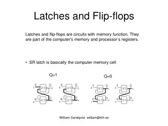
SR (Set/Reset) Latch • SR Latch R N1 Q N2 Q S (S+Q)’ • Consider the four possible cases: § S = 1, R = 0: set output to ‘1’ § S = 0, R = 1: (reset) output to ‘0’ § S = 0, R = 0: store – output should be unchanged § S = 1, R = 1: Trouble! 3
SR Latch Analysis § S = 1, R = 0: 0 R N1 Q 1 N2 Q S § S = 0, R = 1: 1 R N1 Q 0 N2 Q S 4
SR Latch Analysis § S = 0, R = 0: R N1 Q N2 Q S 5
SR Latch Analysis § S = 0, R = 0: R N1 Q N2 Q S What happens if Q prev =0 and Q’ prev =0? A. The output Q toggles B. The output Q remains 0 and Q’ changes to 1 C. The output Q becomes 1 and Q’ remains 0 6
SR Latch Analysis – S = 1, R = 1: 1 R N1 Q 1 N2 Q S 7
Flip-flop Components SR latch (Set-Reset) y S R Q Inputs: S, R State: (Q, y) SR=01, (Q,y) = (0,1) SR=10, (Q,y) = (1,0) SR=11, (Q,y) = (0,0) SR = 00 => if (Q,y) = (0,0) or (1,1), the output keeps toggling 8
Q: Which of the following is a good solution to avoid the output from toggling? A) Avoid the input SR = (0,0) B) Avoid the input SR = (1,1) 9
SR Latch Analysis – S = 0, R = 0: then Q = Q prev and Q = Q prev (memory!) Q prev = 0 Q prev = 1 0 0 R 0 R 1 N1 Q N1 Q 1 0 0 1 1 0 0 N2 Q 0 N2 Q S S – S = 1, R = 1: then Q = 0 and Q = 0 (invalid state: Q ≠ NOT Q ) 1 R 0 N1 Q 0 0 0 1 N2 Q S 10
State table SR Latch Symbol SR inputs 00 01 11 10 PS R Q 0 0 0 X 1 Q(t) 1 1 0 X 1 S Q Q(t+1) NS (next state) Characteristic Expression Q(t+1) = S(t)+R’(t)Q(t) 11
SR Latch Symbol • SR stands for Set/Reset Latch – Stores one bit of state ( Q ) • Control what value is being stored with S , R inputs – Set: Make the output 1 ( S = 1, R = 0, Q = 1 ) – Reset: Make the output 0 ( S = 0, R = 1, Q = 0 ) Must do something to avoid invalid state ( S = R = 1) 12
Clocks 13 Sources: TSR, Katz, Boriello, Vahid, Rosing
Clock question The clock shown in the waveform below has: 1ns CLK A. Clock period of 4ns with 250MHz frequency B. Clock duty cycle 75% C. Clock period of 1ns with 1GHz frequency D. A. & B. E. None of the above 14
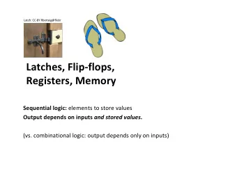
D Latch • Two inputs: CLK , D – CLK : controls when the output changes – D (the data input): controls what the output changes to • Function – When CLK = 1, D passes through to Q (the latch is transparent ) – When CLK = 0, Q holds its previous value (the latch is opaque ) • Avoids invalid case when Q ≠ NOT Q D Latch Symbol CLK D Q Q 15
D Latch Internal Circuit SR Latch Symbol R Q S Q CLK D S R Q Q’ 0 0 0 1 1 0 1 1 16
D Latch Internal Circuit CLK CLK R R Q Q D D Q S S Q Q Q D CLK D D S R Q Q 0 X X 0 0 Q prev Q prev 1 0 1 0 1 0 1 1 1 0 1 0 1 0 17
D Flip-Flop • Two inputs: CLK , D • Function – The flip-flop “samples” D on the rising edge of CLK • When CLK rises from 0 to 1, D passes through to Q • Otherwise, Q holds its previous value – Q changes only on the rising edge of CLK • A flip-flop is an edge-triggered device because it is activated on the clock edge (when CLK rises from 0 1) – D passes through to Q D Flip-Flop Symbols D Q Q 18
D Flip-Flop Internal Circuit • When CLK = 0 CLK – L1 is transparent, L2 is opaque – D passes through to N1 CLK CLK • When CLK = 1 N1 D D Q D Q Q – L2 is transparent, L1 is opaque L1 Q L2 Q Q – N1 passes through to Q 19
Latch and Flip-flop (two latches) CLK A latch can be considered as a door CLK CLK N1 D D Q D Q Q L1 Q L2 Q Q CLK = 0, door is shut CLK = 1, door is unlocked A flip-flop is a two door entrance CLK = 1 CLK = 0 CLK = 1 20
D Flip-Flop vs. D Latch CLK D Q D Q Q Q CLK D Q (latch) Q (flop) 21
D Flip-Flop vs. D Latch CLK D Q D Q Q Q CLK D Q (latch) Q (flop) 22
D Flip-Flop (Delay) Id D Q(t) Q(t+1) Q D 0 0 0 0 1 0 1 0 CLK 2 1 0 1 Q’ 3 1 1 1 State table Characteristic Expression Q(t+1) = D(t) PS D 0 1 0 0 1 What does the equation mean? 1 0 1 NS= Q(t+1) 23
iClicker How long does a D-flip flop store a bit before its output can potentially change? A. Half a clock cycle B. One clock cycle C. Two clock cycles D. There is no minimum time 24
Rising vs. Falling Edge D Flip-Flop D D Q ’ Q ’ Internal design: The triangle Just invert servant Q Q means clock clock rather than input, edge master triggered Symbol for rising-edge Symbol for falling-edge triggered D flip-flop triggered D flip-flop rising edges falling edges Clk Clk 25
Enabled D-FFs • Inputs: CLK , D , EN – The enable input ( EN ) controls when new data ( D ) is stored • Function – EN = 1: D passes through to Q on the clock edge – EN = 0: the flip-flop retains its previous state Internal Circuit Symbol EN CLK 0 D Q Q D Q D 1 EN
27
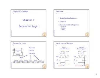
Bit Storage Overview SR latch Level-sensitive SR latch D latch D flip-flop S (set) S D S1 S D latch D latch Q ’ D Dm Qm Ds Qs’ C C Q C m Cs Qs Q Q Q master servant R Clk R R1 R (reset) S=1 sets Q to 1, S and R only have effect SR can’t be 11 if D is Only loads D value present at R=1 resets Q to 0. when C=1. We can stable before and while rising clock edge, so values Problem: SR=11 design outside circuit so C=1, and will be 11 for only can’t propagate to other flip- yield undefined Q. SR=11 never happens a brief glitch even if D flops during same clock cycle. when C=1. Problem: changes while C=1. Tradeoff: uses more gates avoiding SR=11 can be a Problem: C=1 too long internally than D latch, and burden. propagates new values requires more external gates through too many latches: than SR – but gate count is less of an issue today. too short may not enable a store. 28
29
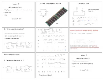
Shift register • Holds & shifts samples of input OUT1 OUT2 OUT3 OUT4 D Q D Q D Q D Q IN CLK 30
Pattern Recognizer • Combinational function of input samples OUT OUT1 OUT2 OUT3 OUT4 D Q D Q D Q D Q IN CLK 31
Counters • Sequences through a fixed set of patterns OUT1 OUT2 OUT3 OUT4 D Q D Q D Q D Q IN CLK 32
Recommend
More recommend
Explore More Topics
Stay informed with curated content and fresh updates.
