Latches, Flip-flops, and Registers Sequential logic: fundamental - PowerPoint PPT Presentation
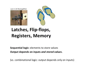
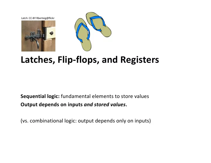
Latch: CC-BY Rberteig@flickr Latches, Flip-flops, and Registers Sequential logic: fundamental elements to store values Output depends on inputs and stored values . (vs. combinational logic: output depends only on inputs) Processor: Data Path
Latch: CC-BY Rberteig@flickr Latches, Flip-flops, and Registers Sequential logic: fundamental elements to store values Output depends on inputs and stored values . (vs. combinational logic: output depends only on inputs)
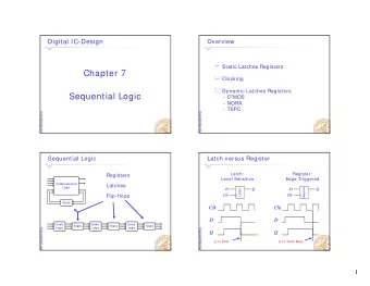
Processor: Data Path Components 1 2 Instruction ALU Registers Memory Fetch and Decode
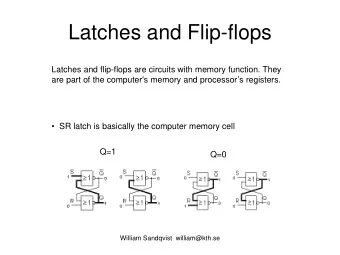
Bistable latches Suppose we somehow get a 1 (or a 0?) on here. Q Q = 0 0 Q Q
SR latch S R Q Q' Q (stable) Q' (stable) 0 0 0 0 ? ? 0 0 0 1 0 1 0 0 1 0 1 0 0 0 1 1 ? ? 1 0 ? ? 1 0 0 1 ? ? 0 1 Set Reset S R Q Q
SR latch Q R Q S R Q R Q Q Q S S S R R Q Q Q Q S
D latch R D Q Data bit Q C S Clock if C = 0 , then SR latch stores current value of Q. if C = 1 , then D flows to Q: if D = 0 , then R = 1 and S = 0, Q = 0 if D = 1 , then R = 0 and S = 1 , Q = 1
Time matters! D C Q
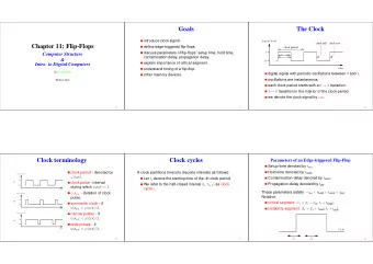
Clocks Clock : free-running signal with fixed cycle time = clock period = T. Clock frequency = 1 / clock period Falling edge Rising edge Clock period A clock controls when to update a sequential logic element's state.
Synchronous systems Inputs to state elements must be valid on active clock edge. State State element Combinational logic element 1 2
D flip-flop with falling-edge trigger leader follower E D Q Q F Q L D F D L D latch D latch Q C F Q F C L Q L C Q next becomes Q now Can still read Q now folower stores E as Q Clock leader stores D as E Time
Time matters! D C E Q
Reading and writing in the same cycle D Q D Flip-Flop Assume Q is initially 0. Clock C Q
D flip-flop = one bit of storage D Q 1 D Flip-Flop C Q
*Half a byte! A 1-nybble* register (a 4-bit hardware storage cell) 0 D Q D Flip-Flop C Q D Q 1 D Flip-Flop C Q 0 D Q D Flip-Flop C Q 1 D Q D Flip-Flop Write C Q Clock
Register file Read register r selector 1 Read register Read data 1 w r selector 2 Read ports Why 2? Read data 2 Write register w r selector Write data w Write port Write? 0 = read 1 = write r = log 2 number of registers w = bits in word Array of registers, with register selectors, write/read control, input port for writing data, output ports for reading data.
Read register number 1 Register 0 Read ports Register 1 M (data out) u . . . Read data 1 x Register n – 2 Register n – 1 Read register number 2 M u Read data 2 x
Write port (data in) write control clock Write C 0 Register 0 1 D . n -to-2 n register number . Register number . decoder C Register 1 n – 2 D n – 1 . . . C Register n – 2 D C Register n – 1 incoming data Register data D
RAM (Random Access Memory) A B Similar to register file, except…
16 x 4 RAM 4-bit address 1101 4 to 16 decoder data out 20
Recommend
More recommend
Explore More Topics
Stay informed with curated content and fresh updates.
