Introduction to FA challenges for Future Technologies: Nanoprobing - PowerPoint PPT Presentation
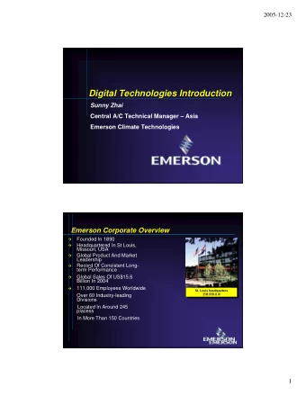
Introduction to FA challenges for Future Technologies: Nanoprobing Key Role Christian Boit TUB Berlin University of Technology, Germany EUFANET Workshop 2008 Maastricht NL Oct 2, 2008 1 Extract of ITRS up to Edition 2007 Perform. Inv.
Introduction to FA challenges for Future Technologies: Nanoprobing Key Role Christian Boit TUB Berlin University of Technology, Germany EUFANET Workshop 2008 Maastricht NL Oct 2, 2008 1
Extract of ITRS up to Edition 2007 Perform. Inv. Delay Materials Approxim. Min phys. Clock On (NMOS Device Year of Feature Chip intrinsic) Concepts Introduction Size [nm] Active Gate Interconn. [GHz] [ps] 1998 120 2.2 12 (2.5) Pocket / SiO 2 Bulk Si Halo Implants 2000 90 2.5 10 (1.8) Cu Poly Low k 2002 65 3.0 9 (1.3) Strain SiGe SOI 2004 45 3.5 8 (1.0) Raised S/D PD Ge S/D 2006 32 4.2 7 (0.8) High k Diel. 2008 23 5.0 5 (0.6) Ultra low k Ultra Thin Ge / III-V Metal Body FD Channels Gates 2010 18 5.8 4 (0.4) Dual Gates More of FIN FETs above 2012 14 6.8 3.5 (0.3) Air? 2014 11 7.9 3 (0.2) Beyond CMOS 2
Optical Backside Circuit Analysis • GHz regime managed by most dynamic techniques Laser Detector • Feature Size Resolution: 2 levels of analysis – Level 1: IR + SIL to Photon identify critical area Emission – Level 2: Nanoprobing to verify critical node – prep circuit destructive LVP increasing need for a high feature resolution probing tool set Laser Stimulated Electrical Signal 3
Nanoprobing (AFP) of Identified Node Detector r ● Resolution < 50nm e s a L ● Parallel lapping down to contact layer Probe ● Isolated devices Tip Tip AFM ● Low ohmic contact Feedback ● Destructive to circuit Additonal Piezo Signals AFP needles tungsten contacts W IMD bulk-Si NW PW bulk Silicon 4
Backside OptiFIB Circuit Edit Contacts to Silicon levels – low risk of charging & of size limitation NW PW FIB deposited Pt n + p + STI p-Poly n-Poly IMD CoSi W M1 5
FIB Backside Trench Procedure ● localized FIB trench ca. 200x200µm 2 Coaxial IR Column: planarity check of trench bottom to chip levels (fringes) - stopping on n-wells - stopping on STI < 400nm remaining Si up to 200x200µm 2 STI Δ Z ≈ 130nm 6
frontside AFP backside ● parallel lapping down ● FIB backside process to contact layer ● devices not isolated ● isolated devices ● creation of new ● low ohmic contact circuit nodes ● Destructive to circuit ● Circuit fully functional AFP needles tungsten FIB Pt contacts D S G W IMD bulk-Si NW PW bulk Silicon 7
UltraThin Si - Ideal Platform for NanoAnalysis Ultra Thin Backside Technique IR Technique Visible or UV Laser Stimulation Dyn. LS Nanoprobing, C-AFM E-Beam Techniques: - Voltage probing LVP, TRE - E Beam induced photocurrent Dyn. LS Nano e - Light Probes n-well STI ≈ 350nm M1 M2 8
Nanoscale Potential Technique Resolution Potential Comment Optical through 500nm 150nm Limited bulk Si (IR) (SIL) resolution Nanoprobing 50nm 10nm Limited dynamics E Beam 100nm 20nm Material degradation? Optical through 300nm < 100nm Realization ultra thin Silicon (SIL) complex UV through ultra 150nm < 50nm Material thin silicon degradation? 9
10
Silicon On Insulator not to etc scale M2 M2 M1 Cu W ILD FuSi STISTI ≅ 0,1µm SiGe p + n + Ge/III-V Ge/III-V ≅ 0,3µm BOX = Buried Oxide Layer ⇒ Silicon On Insulator SOI ≥ 100µm SX ≅ 1,5µm SX 11
Architecture Trends see e.g. T.Skotnicki, short course VLSI 2004 or ITRS roadmap 2003 SOI Silicon On Insulator, PD Partially Depleted, FD Fully Depleted BOX Buried Oxide SON Silicon On Nothing GP Ground Plane 3D ? DG Double Gate 12
Ultra Thin Body UTB SOI: Partially depleted = PD Fully Depleted FD V GS = 0 Poly Deple- BOX Gate ted Si Si Conductive |V GS | > |V T | Channel Subthreshold Slope ≅ 60mV / dec FD active layer ∼ 20nm => UTB 13
Interaction Dimensions • 20nm Gate length Technology • Ultra Thin Silicon UTS (SOI PD) • Ultra thin body UTB (SOI FD / Dual Gate etc) 100nm 20nm 100nm m m n n 50nm 0 50nm 0 2 2 40nm 40nm 14
Recommend
More recommend
Explore More Topics
Stay informed with curated content and fresh updates.
