ICMAB ICMAB INSTITUT DE CINCIA DE INSTITUT DE CINCIA DE MATERIALS - PowerPoint PPT Presentation
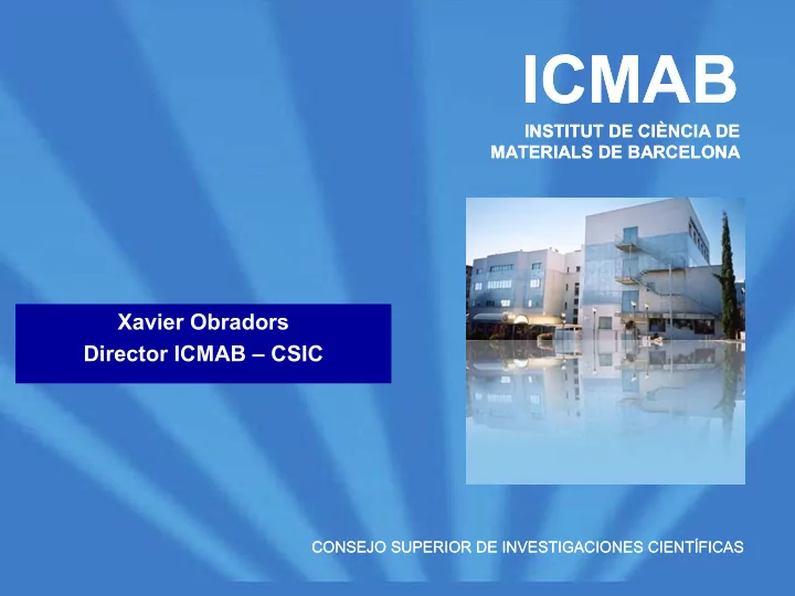
ICMAB ICMAB INSTITUT DE CINCIA DE INSTITUT DE CINCIA DE MATERIALS DE BARCELONA MATERIALS DE BARCELONA Xavier Obradors Director ICMAB CSIC CONSEJO SUPERIOR DE INVESTIGACIONES CIENTFICAS CONSEJO SUPERIOR DE INVESTIGACIONES
ICMAB ICMAB INSTITUT DE CIÈNCIA DE INSTITUT DE CIÈNCIA DE MATERIALS DE BARCELONA MATERIALS DE BARCELONA Xavier Obradors Director ICMAB – CSIC CONSEJO SUPERIOR DE INVESTIGACIONES CIENTÍFICAS CONSEJO SUPERIOR DE INVESTIGACIONES CIENTÍFICAS
Where are we? ALBA SYNCHROTRON Bellaterra campus (Univ. Aut. Barcelona, 20 km)
ICMAB RESEARCH ACTIVITIES
Battery materials High T batteries New materials, alternative mechanisms M x O y + 2y Li + -> y Li 2 O + x M + 2y e - 4.5 Energy Research 250ºC amorphous M x O y 4.0 3 E/V (vs Li) 2,5 3.5 M M % O M M 2 M M M M 3.0 M M M x O y Li 2 O matrix Li 2 O matrix 1,5 2.5 1 nitrides 2.0 0,5 200 150 100 50 0 Capacity (mAh/g) PCT application ES03/00249 0 0 2 4 6 8 10 J. Electrochem. Soc. 152(11), (2005) 'x in Li x Fe 2 O 3 ' Electrochem. Comm. 9, 708 (2007)) Inorg. Chem. (submitted) Correlation microstructure-electrochemical yield β β - β β - -NiOOH -NiOOH NiOOH NiOOH β -Ni(OH) 2 a a c 14 Å 92 Å 92 Å 92 Å ALISTORE ERI b b b b 9.3 Å 9.3 Å Journal of the American Chemical Society, 129, 5840 (2007) Journal of Materials Chemistry 16, 2925 (2006)
Nitride materials with photocatalytical activity in the visible range Nitrogen doping of oxides decreases the band gap because of the lower electronegativity of N vs O, shifting the photocatalytical activity from the UV to the visible range Mesoporous nanostructured thin films New nitrogen doped ceria (CeO 2 ) with Energy Research of TiO 2-x-y N x (anatase) photocatalytical activity in the visible range N1s XPS as a function of the nitriding temperature in NH 3 Solid solution CeO 2-x-y N x up to N bonded to Ti N bonded 4.5 mol % N to Ce Rate of CO 2 evolution for decomposition of acetaldehyde λ as a function of irradiation over N-doped CeO 2 films Rate of CO 2 evolution (ppm/h.cm 2 ) 5 4 3 The mesostructure is kept until 2 T=700 o C 1 0 500 600 300 350 400 450 550 Cut-off wavelength (nm) Chemistry of Materials, 2, 1682 (2008) A.Fuertes, A.B.Jorge. Pat. Esp. 200700482. 23- Advanced Functional Materials, 17, 3348 (2007) 02-2007.
Hydrogen by Ethanol Reforming Catalyst grown on cordierite substrate: Nanocomp- osited silica aerogel with cobalt nanoparticles (blue Energy Research inset) . in the idealized The catalytic device can be simply heated up to the reaction temperature (320-340ºC) under air, and then the ethanol is introduced for the generation of hydrogen. This has a strong potential for fuel cell technology as well as for on-board generation of hydrogen for mobile applications. The catalytic device can be easily operated and doesn’t require special care for shut down cycles, thus allowing interrupted and/or oscillating operation for real practical application. No activation and/or conditioning are required for operation. Co-SiO 2 aerogel-coated catalytic walls for the generation of hydrogen, M.Domínguez, E.Taboada, E.Molins, J.Llorca, Catalysis Today (2008) and CSIC- UPC patent (2007)
Consolider Consolider Chemical solution approaches to self-assembled and nanocomposite superconducting films Xavier Obradors HI PERCHEM T.Puig, A. Pomar, A. Palau, F. Sandiumenge, S. Ricart, N. Mestres, J. Gutiérrez, M. Gibert, A. Llordés, A. Carretero, C. Moreno, R.F. Luccas, J. Zabaleta, F. Martínez, P. Abellán, N. Romà, A. Benedetti, J. Gázquez, M. Coll, R. Vlad, X.Granados Institut de Ciència de Materials de Barcelona, CSIC, 08193 Bellaterra, Spain
POWER APPLICATIONS SUPERCONDUCTORS Transformers 80 Cables FCL 60 T (K) T (K) SMES Motors 40 generators 20 Research NMR Accelerators, MRI Magnets etc 0 0.01 0.1 1 10 100 B (T) B (T)
COATED CONDUCTORS ARCHITECTURE Cap layer : Ag thickness ≈ 0.2 - 0.5 μ m SC layer : YBCO ~ 1.0 μ m Buffer layers : CeO 2 , YSZ, STO,… ~ 0.1 μ m Metallic substrate: RABiTS Ni, SS-IBAD thickness ~ 80 μ m Nanostructure control on km length materials
GOALS • The potentiality and richness of chemical solution methods for growth of nanostructured films and coated conductors: – A flexible, scalable and controllable bottom-up approach • Nanostructured YBCO films by chemical routes – Interfacial nanostructured films – Nanocomposites – Ferromagnetic-superconductor nanostructured YBCO films • Methodology to analyze vortex pinning based on angular dependent transport J c measurements YBCO YBCO Single crystal Single crystal
APS : Artifical Pinning Structures Pinning of vortices by material defects F L = J c x B = F p → v fl = 0 Generation of APS Current flow without dissipation HOW ? J … by nanostructuration The methodology must be versatile, scalable and low cost We choosed a chemical solution route NEED of: • Manipulation, control and tuning of APS • Correlation of nanostructured films with J c • Knowledge on superposition of APS and natural defects • More realistic theoretical pinning models considering complexity
Chemical Solution Deposition … a versatile, scalable and low cost methodology for growth of nanostructured films MOD process For YBCO films … Reacción Reacción Growth Growth Oxygenation Oxigenación Oxigenación Oxygenation Pyrolysis Pyrolysis Pirólisis Pirólisis Spin-coating T T T T on a substrate T 2 T 2 , t T 2 T 2 , t T 3 , t T 3 T 3 , t T 3 Metal-organic - dT 2 /dt - dT 2 /dt T 1 T 1 T 1 T 1 TFA solution dT 1 /dt dT 1 /dt dT 2 /dt dT 2 /dt Epitaxial layer Epitaxial layer - dT 3 / - dT 3 / T(PH T(PH 2 O) 2 O) PO 2 , PH 2 O PO 2 , PH 2 O Gas Flow Gas Flow Gas Flow Gas Flow ω PO 2 , PH 2 O PO 2 , PH 2 O PO 2 , PH 2 O PO 2 , PH 2 O PO 2 , PH 2 O PO 2 , PH 2 O Flujo de Gas Flujo de Gas Coated conductors � Low-cost methodology � High production rate � Scalable to large surfaces � Versatile: nanostructuration
Phase and growth control Film quenched before growth • Intermediate phases: a-Y 2 O 3 ,Y 2 Cu 2 O 5 and CuO embedded in oxyfluorides (OF) • YBCO nucleates exclusively at the interface: island to layer growth J.Gázquez et al, Chem Mat (2006) Y long and winding road: TFA-Y / Ba 1-x Y x F 2 / a-Y 2 O 3 / Y 2 Cu 2 O 5 / Ba 1-x Y x (F,O) 2-y / YBa 2 Cu 3 O 7
Multilayers: Epitaxy and cap layer planarity Ce 1-x [Gd(Zr)] x O 2-y RHEED RHEED High energy IFW-Dresden (00l) facets CZO AFM rms: 3 nm RBS channeling = 12 % (CeO 2 ) χ min χ min = 46 % (CZO) 400nm rms: 0.8nm
Growth of TFA YBCO on MOD CeO 2 cap layers rms roughness is too rough rough rms roughness is too Surface planarity is more useful useful Surface planarity is more nm 0 1 2 3 4 5 µm 4 0 Planarity 2 ) 0.5 3 96,8 % 30 J c (MA/cm 1 2 25 1.5 2 1 20 2.5 0 T = 77K 15 3 3.5 0 1 2 3 4 5 10 4 rms CeO 2 (nm) 5 4.5 5 0 6 6 µm 2 ) 2007 results 2 ) 4 J c (MA/cm 4 J c (MA/cm 2 2 J c (77K)= 5.2 MA/cm 2 T=77K T=77K 0 0 Highest critical current 25 50 75 100 25 50 75 100 % Flat CeO 2 area TFA YBCO on MOD-CeO 2 % Flat CeO 2 area cap layers
Growth of TFA YBCO on MOD-cap metallic substrates YSZ 49% Polycrystalline YBCO (103) substrate/epitaxial multilayer 1 μ m I (a.u.) Δφ (YBCO) =5º Δφ CZO (YSZ) =9.5º Δφ = 5º 76% MOD planarization -8 -4 0 4 8 High SC performances φ (deg) J c (77K)= 1.8 MA/cm 2 1 μ m
Vortex pinning in MOD-YBCO films High quality epitaxial films Island based nucleation and growth J c sf (77K) ~ 4 MA/cm 2 mode → a-b plane defects promotion • Intergrowth • Stacking faults • in-plane partial dislocations Critical current optimization → Correlation nanostructure and vortex pinning at high fields (1- 5T) Pinning defects of specific size and disposition θ Point like defects θ J Linear defects We need to identify and separate different Planar defects vortex pinning contributions
Isotropic and anisotropic pinning defect contributions H//ab H//c c T= 77K F L 1 θ θ θ θ 0.1 a 2 ) J c (MA/cm 0.01 ANISOTROPIC F L 1E-3 defect contribution 1E-4 ISOTROPIC 1E-5 defect contribution 1E-6 Enable to separate ISOTROPIC and 90 135 180 225 ANISOTROPIC defect pinning contributions θ (º) MOD-YBCO, t ≈ 275 nm
J c temperature dependence: Weak and strong pinning Weak pinning − = / ( ) wk T T J T J e 0 0 c c Blatter et al., Rev. Mod. Phys 66 (1994) Strong correlated pinning r 0 < ξ + 2 − = 3 ( / ) ( ) str T T J T J e 0 c c Nelson et al, Phys. Rew. B 48 (1993) PLD-YBCO J.Gutierrez et al., Appl. Phys. Lett. 90 (2007)
Pinning regime diagrams in standard TFA films for H//c Iso-wk Iso-str Aniso-str contribution contribution contribution H irr H irr H irr J anis /J total 8 iso-str total 8 8 8 8 Iso-wk tot J /J J /J c c c c 0,3 c c 0,8 6 6 6 6 6 0,6 0,5 μ 0 H (T) μ 0 H (T) 0,5 μ 0 H (T) 4 4 0.2 4 0,3 4 4 2 2 2 0,4 0.4 2 2 0,2 0.6 0,7 0 0 0 0 0 20 20 40 40 60 60 80 80 0 0 20 20 40 40 60 60 80 80 0 20 40 60 80 Temperature (K) Temperature (K) Temperature (K) 275 nm YBCO-TFA films J. Gutierrez et al, APL 90, 162514 (2007) We have a tool to separate and quantify the three vortex pinning contributions Weak-isotropic defects dominate at low T, strong-isotropic defects at intermediate T and strong-anisotropic defects at high T T.Puig et al., SUST 21, 034008 (2008)
Recommend
More recommend
Explore More Topics
Stay informed with curated content and fresh updates.
