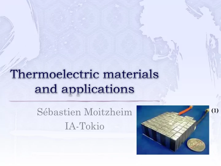

Sébastien Moitzheim (1) IA-Tokio
p n p n Δ T (+) (-) (+) (-) - + Current Sébastien Moitzheim, IA-Tokyo, 2012 3
(1) Sébastien Moitzheim, IA-Tokyo, 2012 4
κ = Thermal conductivity (W m -1 K -1 ) σ = Electrical conductivity ZT ≥ 2 needed for ( Ω cm -2 ) competitiveness α = Seebeck coefficient (1) ( V K -1 ) Figure of merit: Sébastien Moitzheim, IA-Tokyo, 2012 5
Electrical conductivity ↑ Thermal conductivity ↑ ZT ↓ (1) Sébastien Moitzheim, IA-Tokyo, 2012 6
Each material has its own optimal working temperature Choosing the right material for the right application Important factors: Cost Efficiency (2) Stability Sébastien Moitzheim, IA-Tokyo, 2012 7
( ) Denotes research carried out in Japan Source: Thermoelectric Society of Japan, Dr. T. Kajikawa)
Bulk nano-Si Bulk nano-silicon JST- CREST: “ Development of High Efficient Silicon Thermoelectric Materials using Si-nanodeeltjes Nanostructure Control ” 2012 -2017 (¥150M) Ladingstransport Osaka University Warmte wordt geblokkeerd AIST Oxide nanocubes e.g. Strontium Titanate (SrTiO 3 ) JST Project: “ Development of High-Efficiency Thermoelectric Materials and Systems” FY 2007 -2013 (¥227M) Nagoya University Hokkaido University Tokyo University of Science, Yamaguchi AIST Sébastien Moitzheim, IA-Tokyo, 2012 9
1. Use ball-milling to get silicon (Si) particles 2. Oxidize Si particles 3. Etch away SiO 2 4. Use spark plasma sintering (SPS) to form bulk nano-silicon Goal: ZT >1 between RT and 300 °C Sébastien Moitzheim, IA-Tokyo, 2012 10
Recently used to create the best (bulk) thermoelectric material in USA, Nature 2012/09 (ZT = 2.4) However materials used (Lead Tellurium) are toxic Japan wants to use life-friendly and abundant materials World leader in Spark Plasma Sintering (SPS) equipment is Fuji Electronic Industrial (3) Sébastien Moitzheim, IA-Tokyo, 2012 11
Large variety of raw materials can be used Fast process New types of (nanostructured) materials Sébastien Moitzheim, IA-Tokyo, 2012 12
Sébastien Moitzheim, IA-Tokyo, 2012 13
Strontium Titanate (STO) nanocubes Dope with a thin shell of Niobium And a core of Lanthanum 2D electron gas: Many interfaces: high electrical conductivity Low thermal conductivity Sébastien Moitzheim, IA-Tokyo, 2012 14
Sébastien Moitzheim, IA-Tokyo, 2012 15
Recommend
More recommend