Hybrid Go-Kart University of Connecticut Department of Electrical - PowerPoint PPT Presentation
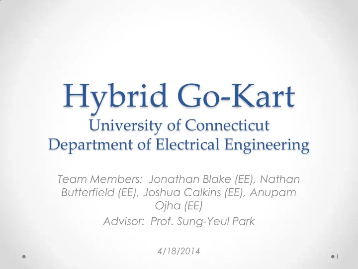
Hybrid Go-Kart University of Connecticut Department of Electrical Engineering Team Members: Jonathan Blake (EE), Nathan Butterfield (EE), Joshua Calkins (EE), Anupam Ojha (EE) Advisor: Prof. Sung-Yeul Park 4/18/2014 1 Outline System
Hybrid Go-Kart University of Connecticut Department of Electrical Engineering Team Members: Jonathan Blake (EE), Nathan Butterfield (EE), Joshua Calkins (EE), Anupam Ojha (EE) Advisor: Prof. Sung-Yeul Park 4/18/2014 1
Outline • System Overview • Flyback Results • PCB Revision • Software • Boost Converter • Budget • Problems Occurred • Final Steps 2
What is Our Project? • Design a power electronics system to combine three separate power sources in order to drive an electric go-kart. 3
The Power Sources • We will use three power sources: o A 30V Lead Acid battery o Four ultra-capacitors, wired in series, at 14V across bank o Photovoltaic Panel, 8->40V output, 200W 4
System Overview 5
System Layout 6
Flyback Schematic
Flyback Specifications • High current caused for multiple design alterations. • 4:7 turns ratio • Voltage Primary 8V-40V. Secondary Voltage 14V. • 16.7% to 50% Duty cycle • Current max 5A in 14.3A • Inductance on primary 20 μ H • 100KHz switching frequency • CCM • Selection of core geometry and material. • Toroid, E I core with gap • Kool m μ , ferromagnetic material, MPP 8
Flyback Results Flyback 25% Duty Cycle 10 Ω Load 25 20 1 − 𝐸)(𝑂 𝑡 𝐸 15 ) 𝑊 𝑝𝑣𝑢 = 𝑊 𝑗𝑜 ( Vout 𝑂 𝑄 10 5 0 0 10 20 30 40 50 Vin • Windings Load Power In Power Out Efficiency 10Ω 2.96W 2.3W 77.70% • DCM 10Ω 12.2W 10.1W 82.80% • Snubber circuit 22Ω 15.6W 14.2W 91% 22Ω 35.1W 34.87W 99.30% • High Power 10Ω 47.3W 40W 84.50% 11Ω 97.7W 68.3W 60.90% • 30.01Vin 17.5Vout 97.2% 5.5Ω 102W 55.9W 54.80% 9
Magnetics 𝑊 𝑞𝑙 𝑢 𝑝𝑜 𝑦10 8 Gauss 𝐶 𝑁𝑏𝑦 = • 𝑂𝐵 𝑓 Core loss due to eddy • currents and hysteresis 𝑋𝑏𝑢𝑢 𝑙 = 𝑙𝑔 𝑛 𝐶 𝑁𝑏𝑦 𝑜 • Core 585 𝐵 𝑀 = 79𝑜𝐼/𝑈 2 • 𝐵 𝑓 = 46.6𝑛𝑛 25 • Saturation 1.05Tesla • 𝐶 𝑁𝑏𝑦 =.107Tesla • Power Loss =3.4W • Wire Loss=2.8W • For 102W input 6.1% • 10
Power Board Layout • Four layer board with 1oz copper with top and bottom layers devoted to low voltage signals. • Combines Flyback converter along with sensing and gate drive circuits for boost converter. 11
Control Board Layout • Texas Instruments DSP TMS320F28335. • Allows up to 6 independently controlled PWM signals. • 8 ADC channels allows for multiple converters to be controlled by single DSP. 12
Power Board Revision • Buck Converter • Non-isolated Output • Flyback Discontinuous mode 13
Software Design • Software being written with Texas Instruments Code Composer v5 to interface with TI DSP. • Software must read the voltage and current values from sensors. • This information will determine the duty ratios for the power converters. • Generate gate switching signal. 14
Control Loop • Current mode control for Boost Converter • PI w/ PV Power Reference for Buck Converter • Danger conditionals 15
ePWM and ADC • ePWM currently active with five signals switching at arbitrary duty ratios at variable frequency. • Due to nature of control board (2 signals per module), interleaving of boost controller limited to two channels always switching at the same time. Cannot interleave four power stages. • ADC and control coding in progress. Awaiting new power board revision to begin debugging. 16
Boost Converter Design • The design of our boost converter has changed drastically. • The driving factor of these changes has been the input current. • Current design is rated for 120A input, with an expected maximum input of 90A. 17
Boost Power-Stage Platform • High-current sections of a boost converter placed on separate platform, connected by cables. • Current and voltage sensor output to microcontroller. • Gate switching would determined by microcontroller, sent through gate drive circuit. 18
Boost Power-Stage Platform (cont.) 19
Budget • Reasons: • PCB $400 X 2 = $800 • Parts = $550 o Power electronics parts • Magnetics = $200 more expense by nature • Mechanical = $30 • Total Spent = $1580 o PCBs have to handle large amounts of current • Total allotted money =$1500 • Over Budget = $-80 20
Problems Encountered • Flyback Efficiency • Large voltage spikes across MOSFETs • Magnetics • Programming took longer than expected 21
Final Steps • Assemble and test Buck Converter • Implement Control Loop Algorithm • Assemble PV Structure 22
Questions? 23
Recommend
More recommend
Explore More Topics
Stay informed with curated content and fresh updates.
