Harry Porters Relay Computer Harry Porter, Ph.D. Portland State - PowerPoint PPT Presentation
Slides to Accompany a Video Tutorial on Harry Porters Relay Computer Harry Porter, Ph.D. Portland State University November 7, 2007 +V Double Throw Relay Double Throw Relay +V Four Pole, Double Throw Relay Four Pole, Double Throw
Slides to Accompany a Video Tutorial on Harry Porter’s Relay Computer Harry Porter, Ph.D. Portland State University November 7, 2007
+V
Double Throw Relay
Double Throw Relay +V
Four Pole, Double Throw Relay
Four Pole, Double Throw Relay +V
Schematic Diagrams Assume other terminal is connected to ground
Schematic Diagrams +V Assume other terminal is connected to ground
The “NOT” Circuit in out 1 out +V 0 in in out 0 1 1 0 Convention: “1” = +12V “0” = not connected
The “NOT” Circuit in out 0 out +V 1 in in out 0 1 1 0 Convention: “1” = +12V “0” = not connected
The “OR” Circuit b b or c c +V b c OUT b 0 0 0 b or c 0 1 1 1 0 1 1 1 1 +V c
An Optimization? b b b or c c b or c c
An Optimization? b b b or c b or c c c or d c d c or d d
An Optimization? b b b or c b or c c c or d c d c or d d Whoops!
An Optimization? b b b or c b or c c +V c or d c or d c d d
1-Bit Logic Circuit b c NOT AND OR XOR 0 0 1 0 0 0 0 1 1 0 1 1 1 0 0 0 1 1 1 1 0 1 1 0 NOT b AND OR c XOR
1-Bit Logic Circuit b c NOT AND OR XOR 0 0 1 0 0 0 0 1 1 0 1 1 1 0 0 0 1 1 V 1 1 0 1 1 0 NOT b AND OR c XOR
1-Bit Logic Circuit b c NOT AND OR XOR 0 0 1 0 0 0 0 1 1 0 1 1 1 0 0 0 1 1 V 1 1 0 1 1 0 NOT b AND OR c XOR
1-Bit Logic Circuit b c NOT AND OR XOR 0 0 1 0 0 0 0 1 1 0 1 1 1 0 0 0 1 1 V 1 1 0 1 1 0 NOT b AND OR c XOR
1-Bit Logic Circuit b c NOT AND OR XOR 0 0 1 0 0 0 0 1 1 0 1 1 1 0 0 0 1 1 V 1 1 0 1 1 0 NOT b AND OR c XOR
1-Bit Logic Circuit b c NOT AND OR XOR 0 0 1 0 0 0 0 1 1 0 1 1 1 0 0 0 1 1 V 1 1 0 1 1 0 NOT b AND OR c XOR
Eight 1-bit circuits can be combined to build an... 8-Bit Logic Circuit B7 C7 B1 C1 B0 C0 Logic Logic Logic • • • Circuit Circuit Circuit XOR 1 XOR 0 XOR 7 OR 1 OR 0 OR 7 AND 1 AND 0 AND 7 NOT 1 NOT 0 NOT 7
The “Full Adder” Circuit Cy in B C Cy out Sum B C 0 0 0 0 0 0 0 1 0 1 Carry out Carry in 0 1 0 0 1 Full 0 1 1 1 0 Adder 1 0 0 0 1 1 0 1 1 0 1 1 0 1 0 Sum 1 1 1 1 1
8 full-adders can be combined to build an... 8-Bit Adder B 7 C 7 B 1 C 1 B 0 C 0 Carry Carry Carry Full Full Full 0 • • • Adder Adder Adder Sum 7 Sum 1 Sum 0 8 B 8 Sum + 8 Carry C
The Zero-Detect Circuit Zero V+ Result Bus
The Zero-Detect Circuit Zero V+ Result Bus Sign
Enable Circuit Enable
B XOR C Enable Circuit x 7 x 6 x 5 x 4 x 3 x 2 x 1 x 0 Enable Result Bus
B Shift Left Circular (SHL) b 7 b 6 b 5 b 4 b 3 b 2 b 1 b 0 Enable Result Bus
3-to-8 Decoder f 0 f 1 f 2 OUTPUT 0 0 0 1 0 0 0 0 0 0 0 0 0 1 0 1 0 0 0 0 0 0 0 1 0 0 0 1 0 0 0 0 0 0 1 1 0 0 0 1 0 0 0 0 1 0 0 0 0 0 0 1 0 0 0 1 0 1 0 0 0 0 0 1 0 0 1 1 0 0 0 0 0 0 0 1 0 1 1 1 0 0 0 0 0 0 0 1 ADD INC AND OR XOR NOT V SHL f 0 <unused> f 1 f 2
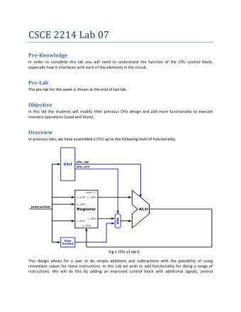
Arithmetic Logic Unit (ALU) B 8 C 8 Function 3 8-bit 8-bit Adder Logic ADD SHL INC AND XOR NOT OR 3-to-8 Decoder Enable En En En En En En Data Bus 8 Zero-Detect Sign Carry Zero
An 8-Bit ALU 3 Function Code 000 add 001 inc 010 and 8 B 011 or 8 Result 100 xor ALU 101 not 110 shl 8 C 111 <nop> Carry Sign Zero
Register Storage +V A
Register Storage • • • +V A 7 A 6 A 0
Register Storage • • • +V A 7 A 6 A 0 Select Enable Bus
Register Storage • • • A 7 A 6 A 0 Load Select Enable Bus
Register Storage • • • A 7 A 6 A 0 Load Select Enable Bus
8-Bit Registers “Y” Register “X” Register Load Load Select Select 8-Bit “Data” Bus
16-Bit “Address” Bus Load Select “Y” Register “X” Register Load Load Select Select 8-Bit “Data” Bus
A B 8-bit ALU C D Z Cy S M 1 M M 2 8-bit Data Bus X XY 16-bit Address Bus Y System J 1 J J 2 Architecture Inst PC Inc 16-bit Increment Memory Addr Data
32K Byte Static RAM Chip LEDs 8 FET Power Transistors (to drive relays during a memory-read operation)
A B 8-bit ALU C D Z Cy S M 1 M M 2 8-bit Data Bus X 16-bit Address Bus XY Y Example: J 1 J J 2 The ALU Inst PC Instruction Inc 16-bit Increment Memory Addr Data
A B 8-bit ALU C D Z Cy S M 1 M M 2 8-bit Data Bus X 16-bit Address Bus XY Step 1: Y J 1 J Fetch Instruction J 2 Inst PC LOAD Inc MEM-READ SELECT 16-bit Increment Memory Addr Data
A B 8-bit ALU C D Z Cy S M 1 M M 2 8-bit Data Bus X 16-bit Address Bus XY Step 2: Y J 1 J Increment PC J 2 Inst PC Inc SELECT 16-bit LOAD Increment Memory Addr Data
A B 8-bit ALU C D Z Cy S M 1 M M 2 8-bit Data Bus X 16-bit Address Bus XY Y Step 3: J 1 J J 2 Update PC Inst PC Inc LOAD 16-bit SELECT Increment Memory Addr Data
A B 8-bit ALU C LOAD D Z Cy S M 1 M LOAD M 2 FUNCTION 8-bit Data Bus X 16-bit Address Bus XY Y J 1 J Step 4: J 2 Inst Execute Instruction PC Inc 16-bit Increment Memory Addr Data
Clock +V Output Switch +V
Clock +V Output Switch +V Charging
Clock +V Output Switch +V Discharging
Clock +V Output Switch +V
Clock +V +V +V +V A B C D
Clock On On +V +V +V +V A B C D Discharging Charging
Clock On On +V +V +V +V A B C D Discharging Charging
Clock On On +V +V +V +V A B C D Discharging Charging
Clock On On +V +V +V +V A B C D Discharging Charging
Clock On On +V +V +V +V A B C D Discharging Charging
Clock Timing Diagram A B C D Clock Clock = (A and B) or (C and D)
Finite State Machine clock 1 2 3 4 5 6 7 8 t 1 t 2 t 3 t 4 t 5 t 6 t 7 t 8 Outputs
Output from FSA 1 2 3 4 5 6 7 8 1 2 3 4 5 6 7 8 1 2 3 t 1 t 2 t 3 t 4 t 5 t 6 t 7 t 8
Instruction Timing - ALU Instruction 1 2 3 4 5 6 7 8 1 2 3 4 5 6 7 8 1 2 3 Select PC Memory Read Load Instr Load Inc Select Inc Load PC ALU Function Load A Load Cond.Code Reg.
Instruction Timing - ALU Instruction 1 2 3 4 5 6 7 8 1 2 3 4 5 6 7 8 1 2 3 Select PC Fetch Memory Read Load Instr Load Inc Select Inc Load PC ALU Function Load A Load Cond.Code Reg.
Instruction Timing - ALU Instruction 1 2 3 4 5 6 7 8 1 2 3 4 5 6 7 8 1 2 3 Select PC Increment Memory Read Load Instr Load Inc Select Inc Load PC ALU Function Load A Load Cond.Code Reg.
Instruction Timing - ALU Instruction 1 2 3 4 5 6 7 8 1 2 3 4 5 6 7 8 1 2 3 Select PC Memory Read Load Instr Load Inc Select Inc Execute Load PC ALU Function Load A Load Cond.Code Reg.
Instruction Decoding Finite State Machine Instruction Register • • • 7 6 5 4 3 2 1 0 1 2 3 4 5 6 Combinational Logic Control Signals (Load, Select, Mem-Read, etc.)
Instruction Timing - 16-bit Move 1 2 3 4 5 6 7 8 1 2 3 4 5 6 7 8 9 10 1 Select PC (Same as Memory Read before) Load Instr Load Inc Select Inc Load PC Select Source-Register Load Dest-Register
Finite State Machine 1 2 3 4 5 6 7 8 9 10 11 12 13 14 15 16 17 18 19 20 21 22 23 24
Instruction Decoding and Control Clock Data Bus Finite State Instruction Machine Register Instruction Decoding Control Lines
The Instruction Set Move ddd = destination register sss = source register 0 0 d d d s s s (A, B, C, D, M 1 ,M 2 ,X or Y) ALU r = destination register (A or D) 1 0 0 0 r f f f fff = function code (add, inc, and, or, xor, not, shl) Load Immediate r = destination register (A or B) ddddd = value (-16..15) 0 1 r d d d d d 16-bit Increment XY ← XY + 1 1 0 1 1 0 0 0 0
The Instruction Set Load rr = destination register (A, B, C, D) reg ← [M] 1 0 0 1 0 0 r r Store rr = source register (A, B, C, D) 1 0 0 1 1 0 r r [M] ← reg Load 16-bit Immediate 1 1 0 0 0 0 0 0 v v v v v v v v v v v v v v v v Load the immediate value into M (i.e., M 1 and M 2 ) Halt 1 0 1 0 1 1 1 0
The Instruction Set Goto 1 1 1 0 0 1 1 0 a a a a a a a a a a a a a a a a Branch to the given address Call 1 1 1 0 0 1 1 1 a a a a a a a a a a a a a a a a Branch to the given address Save return location in XY register Return / Branch Indirect PC ← XY 1 0 1 0 1 0 1 0 16-Bit Move d = destination register (PC or XY) ss = source register (M, XY or J) 1 0 1 0 d s s 0
Recommend
More recommend
Explore More Topics
Stay informed with curated content and fresh updates.


