Hardware Design with VHDL Design Example: UART ECE 443 UART - PowerPoint PPT Presentation
Hardware Design with VHDL Design Example: UART ECE 443 UART Universal Asynchronous Receiver and Transmitter A serial communication protocol that sends parallel data through a serial line. Typically used with RS-232 standard. Your FPGA boards
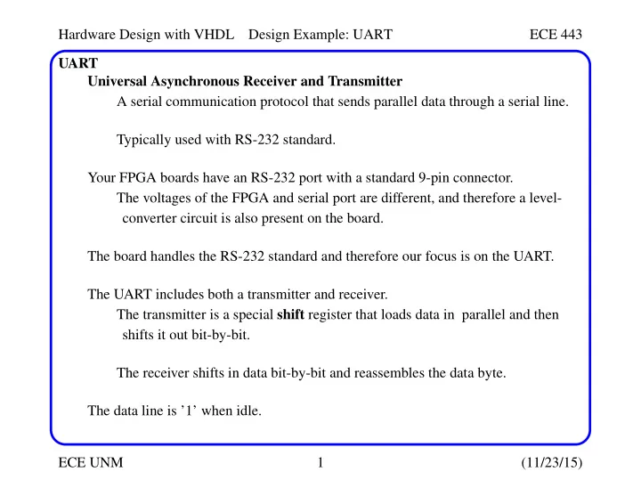
Hardware Design with VHDL Design Example: UART ECE 443 UART Universal Asynchronous Receiver and Transmitter A serial communication protocol that sends parallel data through a serial line. Typically used with RS-232 standard. Your FPGA boards have an RS-232 port with a standard 9-pin connector. The voltages of the FPGA and serial port are different, and therefore a level- converter circuit is also present on the board. The board handles the RS-232 standard and therefore our focus is on the UART. The UART includes both a transmitter and receiver. The transmitter is a special shift register that loads data in parallel and then shifts it out bit-by-bit. The receiver shifts in data bit-by-bit and reassembles the data byte. The data line is ’1’ when idle. ECE UNM 1 (11/23/15)
Hardware Design with VHDL Design Example: UART ECE 443 UART Spec Transmission starts when a start bit (a ’0’) is sent, followed by a number of data bits (either 6, 7 or 8), an optional partity bit and stop bits (with 1, 1.5 or 2 ’1’s). idle start stop d7 d6 d5 d4 d0 d2 d3 d1 This is the transmission of 8 data bits and 1 stop bit. Note that no clk signal is sent through the serial line. This requires agreement on the transmission parameters by both the transmitter and receiver in advance. This information includes the band rate (number of bits per second), the num- ber of data bits and stop bits, and whether parity is being used. Common baud rates are 2400, 4800, 9600 and 19,200. ECE UNM 2 (11/23/15)
Hardware Design with VHDL Design Example: UART ECE 443 UART Receiving Subsystem An oversampling scheme is commonly used to locate the middle position of the trans- mitted bits, i.e., where the actual sample is taken. The most common oversampling rate is 16 times the baud rate. Therefore, each serial bit is sampled 16 times but only one sample is saved as we will see. The oversampling scheme using N data bits and M stop bits: • Wait until the incoming signal becomes ’0’ (the start bit) and then start the sampling tick cnter. • When the cnter reaches 7, the incoming signal reaches the middle position of the start bit. Clear the cnter and restart. • When the cnter reaches 15, we are at the middle of the first data bit. Retrieve it and shift into a register. Restart the cnter. • Repeat the above step N-1 times to retrieve the remaining data bits. • If optional parity bit is used, repeat this step once more. • Repeat this step M more times to obtain the stop bits. ECE UNM 3 (11/23/15)
Hardware Design with VHDL Design Example: UART ECE 443 UART Receiving Subsystem The oversampling scheme replaces the function of the clock. Instead of using the rising edge to sample, the sampling ticks are used to esti- mate the center position of each bit. Note that the system clock must be much faster than the baud rate for oversampling to be possible. The receiver block diagram consists of three components rx d_out r_data d_out rx clk rx_done_tick rd_uart s_tick rx_empty tick interface UART baud receiver circuit rate generator The interface circuit provides a buffer and status between the UART and the com- puter or FPGA. ECE UNM 4 (11/23/15)
Hardware Design with VHDL Design Example: UART ECE 443 UART Receiving Subsystem The baud rate generator generates a sampling signal whose frequency is exactly 16 times the UART’s designated baud rate. To avoid creating a new clock domain, the output of the baud rate generator will serve to enable ticks within the UART rather than serve as the clk signal. The whole system will use one clk as we will see. For a 19,200 baud rate, the sampling rate has to be 307,200 (19,200*16) ticks per second. With a system clk at 50 MHz, the baud rate generator need a mod-163 cnter (50 MHz/307,200). Therefore, the tick output will assert for one clk cycle every 163 clk cycles of the system clk. The following code from page 83 of the text can be used to implement a mod-163 cnter. ECE UNM 5 (11/23/15)
Hardware Design with VHDL Design Example: UART ECE 443 UART Receiving Subsystem: mod-163 cnter library ieee; use ieee.std_logic_1164. all ; use ieee.numeric_std. all ; entity mod_m_cnter is generic ( N: integer := 4; M: integer := 10; ); port ( clk, reset: in std_logic; max_tick: out std_logic; q: out std_logic_vector(N-1 downto 0); ); end mod_m_cnter; architecture arch of mod_m_cnter is signal r_reg: unsigned(N-1 downto 0); signal r_next: unsigned(N-1 downto 0); ECE UNM 6 (11/23/15)
Hardware Design with VHDL Design Example: UART ECE 443 UART Receiving Subsystem: mod-163 cnter begin process (clk, reset) begin if (reset = ’1’) then r_reg <= ( others => ’0’); elsif (clk’event and clk=’1’) then r_reg <= r_next; end if ; end process ; end arch; -- next state logic r_next <= ( others => ’0’) when r_reg=(M-1) else r_reg + 1; -- output logic q <= std_logic_vector(r_reg); max_tick <= ’1’ when r_reg=(M-1) else ’0’; end arch; ECE UNM 7 (11/23/15)
Hardware Design with VHDL Design Example: UART ECE 443 UART Receiving Subsystem: UART receiver The ASMD chart for the receiver is shown below: idle data stop F F F rx = 0 s_tick=1 s_tick=1 F F s=15 s=SB_TICK-1 s <= 0 s <= s+1 start s <= s+1 s <= 0 F rx_done_tick <= 1 b <= rx&(b>>1) s_tick=1 F F s=7 n=D_BIT-1 s <= s+1 s <= 0 states: idle, start, data, stop n <= n+1 n <= 0 s_tick is enable tick from baud generator. D_BIT indicates the number of data bits and SB_TICK indicates the number of ticks needed for the stop bits (16, 24 and 32 for 1, 1.5 and 2 stop bits). ECE UNM 8 (11/23/15)
Hardware Design with VHDL Design Example: UART ECE 443 UART Receiving Subsystem: UART receiver We will assign D_BIT and SB_TICK to 8 and 16, respectively, in our design. library ieee; use ieee.std_logic_1164. all ; use ieee.numeric_std. all ; entity uart_rx is generic ( DBIT: integer := 8; SB_TICK: integer := 16; ); port ( clk, reset: in std_logic; rx: in std_logic; s_tick: in std_logic; rx_done_tick: out std_logic; dout: out std_logic_vctor(7 downto 0) ); end uart_rx; ECE UNM 9 (11/23/15)
Hardware Design with VHDL Design Example: UART ECE 443 UART Receiving Subsystem: UART receiver architecture arch of uart_rx is type state_type is (idle, start, data, stop); signal state_reg, state_next: state_type; signal s_reg, s_next: unsigned(3 downto 0); signal n_reg, n_next: unsigned(2 downto 0); signal b_reg, b_next: std_logic_vector(7 downto 0); begin process (clk, reset) -- FSMD state and data regs. begin if (reset = ’1’) then state_reg <= idle; s_reg <= ( others => ’0’); n_reg <= ( others => ’0’); b_reg <= ( others => ’0’); elsif (clk’event and clk=’1’) then state_reg <= state_next; s_reg <= s_next; n_reg <= n_next; ECE UNM 10 (11/23/15)
Hardware Design with VHDL Design Example: UART ECE 443 UART Receiving Subsystem: UART receiver b_reg <= b_next; end if ; end process ; -- next state logic process (state_reg, s_reg, n_reg, b_reg, s_tick, rx) begin state_next <= state_reg; s_next <= s_reg; n_next <= n_reg; b_next <= b_reg; rx_done_tick <= ’0’; case state_reg is when idle => if (rx = ’0’) then state_next <= start; s_next <= ( others => ’0’); end if ; ECE UNM 11 (11/23/15)
Hardware Design with VHDL Design Example: UART ECE 443 UART Receiving Subsystem: UART receiver when start => if (s_tick = ’1’) then if (s_reg = 7) then state_next <= data; s_next <= ( others => ’0’); n_next <= ( others => ’0’); else s_next <= s_reg + 1; end if ; end if ; when data => if (s_tick = ’1’) then if (s_reg = 15) then s_next <= ( others => ’0’); b_next <= rx & b_reg(7 downto 1); if (n_reg = (DBIT - 1)) then state_next <= stop; else ECE UNM 12 (11/23/15)
Hardware Design with VHDL Design Example: UART ECE 443 UART Receiving Subsystem: UART receiver n_next <= n_reg + 1; end if ; else s_next <= s_reg + 1; end if ; end if ; when stop => if (s_tick = ’1’) then if (s_reg = (SB_TICK-1)) then state_next <= idle; rx_done_tick <= ’1’; else s_next <= s_reg + 1; end if ; end if ; end case ; end process ; dout <= b_reg; end arch; ECE UNM 13 (11/23/15)
Hardware Design with VHDL Design Example: UART ECE 443 UART Receiving Subsystem: Interface Circuit The receiver interface circuit has two functions: • It provides a mechanism to signal the availability of a new word • It provides buffer space between the receiver and main system. Several architectures are possible, including one with a FIFO. Here is one with a flag FF (to indicate the reception of a data byte) and a one byte buffer. rx q d_out r_data d_out rx clk rd_uart rx_done_tick en s_tick register tick UART rx_empty baud receiver set_flag flag rate clr_flag generator rd_uart register Here, rx_done_tick is connected to set_flag while the system connects to clr_flag . The system checks rx_empty to determine when a data byte is available. ECE UNM 14 (11/23/15)
Recommend
More recommend
Explore More Topics
Stay informed with curated content and fresh updates.
