Graphene heterostructures: electronic properties and potential - PowerPoint PPT Presentation
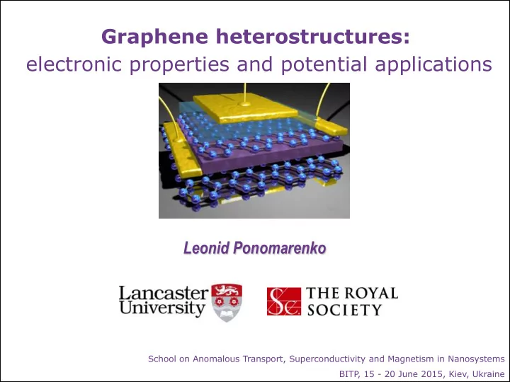
Graphene heterostructures: electronic properties and potential applications Leonid Ponomarenko School on Anomalous Transport, Superconductivity and Magnetism in Nanosystems BITP , 15 - 20 June 2015, Kiev, Ukraine Graphene Graphite: strong
Graphene heterostructures: electronic properties and potential applications Leonid Ponomarenko School on Anomalous Transport, Superconductivity and Magnetism in Nanosystems BITP , 15 - 20 June 2015, Kiev, Ukraine
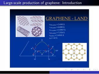
Graphene Graphite: strong in-plane bonding weak inter-plane interaction Graphene was isolated and measured for the first time in 2004 Geim Novoselov The Nobel Prize in Physics 2010 was awarded jointly to Andre Geim and Konstantin Novoselov " for groundbreaking experiments regarding the two-dimensional material graphene "
Graphene Superlatives thinnest imaginable material strongest material ever measured stiffest known material (stiffer than diamond) most stretchable crystal (up to 20% elastically) record thermal conductivity (outperforming diamond) highest current density at room T (million times of those in copper) highest intrinsic mobility (100 times more than in Si) lightest charge carriers (zero rest mass) longest mean free path at room T (micron range) most impermeable (even He atoms cannot squeeze through) ...
National Graphene Institute • £61M building funded by UK Government and European Union Prof V. Fal’ko , • Officially opened in March 2015 director of NGI (from 8/06/15)
Graphene is not alone MoS 2 NbSe 2 Boron-Nitride Graphene GraFane Graphane Van der Waals heterostructures. Geim & Grigorieva, NATURE (2013)
Outline Properties of graphene monolayer band structure field effect Graphene – BN heterostructures fabrication superlattices Hofstadter butterfly SiO 2 Si graphene Graphene multilayer structures metal-insulator transition Coulomb drag tunnelling transistors
Outline Properties of graphene monolayer band structure field effect Graphene – BN heterostructures fabrication 10 m superlattices Hofstadter butterfly Graphene multilayer structures metal-insulator transition Coulomb drag tunnelling transistors
Outline Properties of graphene monolayer band structure field effect Graphene – BN heterostructures fabrication superlattices Hofstadter butterfly Graphene multilayer structures metal-insulator transition Coulomb drag tunnelling transistors
Band Structure and Field Effect tight binding calculations, Phil Wallace, Phys. Rev. 71, 622 (1947) Hexagonal lattice, A-B sublattice symmetry (= inversion symmetry) SiO 2 Si graphene 0.25 eV Geim & Novoselov, Science 2004 Mechanical exfoliation (“Sticky tape” method)
Band Structure and Field Effect B B – magnetic field Hall en n – carrier density 1 en µ - mobility 10 000 cm 2 /Vs (on SiO2) 1 000 000 cm 2 /Vs (suspended, 4 K) SiO 2 Si graphene Geim & Novoselov, Science 2004 Mechanical exfoliation (“Sticky tape” method)
On/Off Ratio End of Introduction Part 2 things to remember: Graphene is always conducting; FET doesn’t work. OFF In graphene ON/OFF ratio is ~ 20 at room T (needed ~ 10 3 for FET) there is no proper OFF state because of zero band gap ON
Graphene Heterostructures Boron nitride substrates for high-quality graphene electronics C. R. Dean et al. Nature Nano 5, 722 (2010) One order improvement in mobility . Fractional Quantum Hall Effect Dean et al., Nature Phys . (2011)
Different forms of Boron Nitride Hexagonal – Cubic – almost as Fullerene-like BN nanotubes “white graphite” hard as diamond molecule B 12 N 12 Graphene Boron Nitride BN: insulator with gap 5.8 eV K. Watanabe et al, Nature Materials 2004. Inversion symmetry is broken! a = 2.462 A, c = 6.708 A a = 2.504 A, c = 6.661 A
Dry-peel transfer
Bubbles everything covered optics SEM with contamination TEM 20 m 2 nm AFM AFM occasional 10 nm scale patches 0.5 m 2 nm so much contamination BUBBLES
Mobility and Mean Free Path
Mobility and Mean Free Path The width of the Hall bar is 2 m At low temperatures the MFP is limited by the size of the device
graphene-hBN interface in TEM SEM 10 m NO CONTAMINATION LAYER at the interface between graphene & hBN chemical TEM analysis Focused ion beam (FIB) milling + STEM Slices 20-70 nm thick Manchester, Nature Materials 2012
moiré patterns: graphene on hBN periodicity =2.4 nm 6.0 nm 11.5 nm Yankowitz et al, Nature Phys 2012 Xue et al, Nature Mat 2011; Decker et al, Nanolett 2011 Scanning tunnelling microscopy (STM): • the period is much larger than graphene lattice constant • conductance electrons “feel” periodic potential
Graphene on Substrate with Similar Lattice Constant Moiré pattern: well defined long range order Graphene is just one atom thick. Electrons feel atoms of the substrate (if the interface is clean) What happens in strong magnetic field?
moiré patterns: graphene on hBN periodicity =2.4 nm 6.0 nm 11.5 nm Yankowitz et al, Nature Phys 2012 Xue et al, Nature Mat 2011; Decker et al, Nanolett 2011 𝐹 𝑡 THEORY: Steve Louie‘s group Nature Phys 2008, PRL 2008 Francois Peeters ’ group PRB 2010-2012 Burset et al, PRB 2011 Ortix et al, PRB 2012 Kindermann et al, PRB 2012 −𝐹 𝑡 Fal’ko et al, PRB 2013 and SOME MORE
moiré patterns: graphene on hBN periodicity =2.4 nm 6.0 nm 11.5 nm Yankowitz et al, Nature Phys 2012 𝐹 𝑡 New Dirac points generated at the edges of the superlattice Brillouin zone −𝐹 𝑡
can we probe in transport? periodicity =2.4 nm 6.0 nm 11.5 nm need moiré like this Yankowitz et al, Nature Phys 2012 𝐹 𝑡 = 2𝜌ℏ𝑊F 3 𝜇 𝐹 𝑡 for short periods, gaps lie at too high energies <2 degrees accessible by the field effect “invisible” for transport −𝐹 𝑡 measurements
specially aligned graphene devices ambient CAFM: moiré in graphene on BN with 12 nm period
secondary Dirac points specially aligned graphene devices new neutrality points @0.2-0.35 eV electron-like orbits for strong hole doping and vice versa n~3x10 12 cm -2 , = 13 nm, (A = 150 nm 2 ) 4 electrons/u.c. second generation Dirac fermions Ponomarenko et al. Nature (2013)
what happen in magnetic field? Two competing lengthscales: a : lattice periodicity l B : magnetic length Duglas F. Hofstadter, Phys. Rev. B 14, 2239 (1976) flux quanta per unit cell Energy levels develop fractal structure when magnetic length is of the order ⅕ ¼ ⅓ ½ / 0 0 1 of the lattice period graphene: graphene/BN superlattice: ≈ 14 nm A ≈ 170 nm 2 B ≈ 24 T ( / 0 = 1) a ≈ 0.25 nm ⇒ B ≈ 10 4 T
Tracing gaps in B and n n/n 0 / 0 / 0 0 1 0 1 Hofstadter’s energy spectrum Wannier diagram Phys. Status Solidi 88 , 757 (1978) gaps are constrained to linear trajectories in the B-n diagram: n t s t , s ℤ n 0 0 n/n 0 – normalised density (n 0 = 4/A, where A is the area of supercell)
Glimpse of Hofstadter’s butterfly Earlier attempts in GaAs based structures T. Schlosser et al, Semicond. Sci. Technol. (1996) C. Albrecht et al, PRL (2001) M. C. Geisler et al, PRL (2004) T. Schlosser et al, Europhys. Lett.(1996) • Large unit cell (100 nm or larger) • Limited range of densities • Significant disorder
Magnetotransport measurements Some of the features of Hofstadter’s energy spectrum are seen in magnetotransport “Landau levels” fanning from the secondary DP 𝐹 𝑀𝑀 (12 𝑈) > Δ 𝑤𝐼 L. A. Ponomarenko et al. Nature 497, 594 – 597 (2013) C. R. Dean et al. Nature 497, 598 – 602 (2013) B. Hunt et al., Science 340, 1427-1430 (2013)
Capacitance Measurements Simple and reliable technique for 𝐷 = 𝜁𝜁 0 𝑊 = 𝐹𝑒 = 𝑓𝑜 𝑊 𝒆 𝑒 , studying details of the band structure 𝐷 “geometrical” capacitance 𝑊 = 𝐹𝑒 + 1 𝑊 𝑊 ∝ 𝑜 𝑓 𝜈(𝑜) 𝐷 𝑟 = 𝑓 2 𝑒𝑜 𝐷 = 1 1 + 1 𝑒𝜈 𝐷 𝐷 𝑟 density of states L.A.Ponomarenko et al, PRL 105 136801 (2010)
Signature of Hofstadter’s butterfly Black – Landau fan (4x degenerate) Blue – Landau fan (degeneracy lifted, QHFM) Green – “Landau levels” from secondary DPs Red – gaps in Hofstadter spectrum G.L.Yu et al. Nature Physics 10, 525 (2014)
Conclusions for Part 2 Graphene superlattice is an excellent example of “band structure engineering” and creating artificial structures with on demand properties (simply by controlling the orientation of graphene with respect to the properly chosen substrate) Hofstadter butterfly has been finally observed (almost 40 years after its prediction)
Graphene Double Layer Structures Layer-by-layer material engineering BN-Gr-BN-Gr-BN BN thickness: B 50,000 to 120,000 cm 2 /Vs anything down to monolayer T 30,000 to 60,000 cm 2 /Vs (drag measurements - 3 layers) High quality, perfect interface, versatile system
Double Layer Structures GaAs/AlGaAs double-quantum-well structures have been studied for more than 20 years (in particular J. Eisenstein group, Caltech) also Cavendish and Sandia Labs on e-h bilayers T.J. Gramila et al, Phys. Rev. Lett. (1991) Weakly coupled layers (d<<n -1/2 ): e-e scattering (Coulomb drag) Strongly coupled layers: support coherent state (excitonic condensation) Tunnelling spectroscopy: details of bend structure
Recommend
More recommend
Explore More Topics
Stay informed with curated content and fresh updates.
