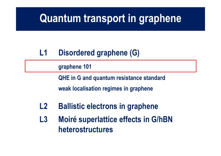
Quantum transport in graphene L1 Disordered graphene (G) graphene - PowerPoint PPT Presentation
Quantum transport in graphene L1 Disordered graphene (G) graphene 101 QHE in G and quantum resistance standard weak localisation regimes in graphene L2 Ballistic electrons in graphene L3 Moir superlattice effects in G/hBN
Quantum transport in graphene L1 Disordered graphene (G) graphene 101 QHE in G and quantum resistance standard weak localisation regimes in graphene L2 Ballistic electrons in graphene L3 Moiré superlattice effects in G/hBN heterostructures
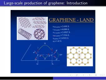
2 sp hybridisation forms strong directed covalent bonds between carbons (at 120 o ) which determine the honeycomb lattice structure C � - bonds � � * empty 2 sp p z -bands � 2 sp full
Graphenes Exfoliated from bulk graphite onto a substrate, or hanged suspended (highest quality G/hBN in L2, L3) Grown using chemical vapor deposition (CVD) on metals (Cu, Ni), or insulators: polycrystalline and strained Epitaxial graphene sublimated on Si-terminated surface of SiC: wafer-scale single-crystalline carpet
Wallace, Phys. Rev. 71, 622 (1947) Slonczewski, Weiss, Phys. Rev. 109, 272 (1958) � ~ 3 eV 0
Wallace, Phys. Rev. 71, 622 (1947) Slonczewski, Weiss, Phys. Rev. 109, 272 (1958)
First � Brillouin e � 2 � i / 3 zone i 0 e 2 � i / 3 e � Valley G Valley � G '
� � � � � a a a a a � i ( p p ) i p � i ( p p ) � 2 2 i i � � � � � H e e x y e y e e x y 2 2 2 3 3 2 3 3 3 � � � � AB , K 0 � � � � 3 a ( p ip ) 0 x y 2 � � � � 3 H a ( p ip ) BA , K 0 x y 2 Bloch function amplitudes (e.g., in the valley K) on the AB sites (‘isospin’) mimic spin components of a massless relativistic particle. � � � � � � A � � � � � � B � � � 0 p ip � � � ˆ � � x y � � � � � H v v p � � � � p ip 0 p � � x y � � 8 3 v a ~ 10 cm McClure, PR 104, 666 (1956) 0 2 sec
� � � � � H v p � p � � p � ( p cos , sin ) Bloch function amplitudes on the A/B sites Wave function. sublattice composition � � � � � � � � B � � is linked to the axis � A � � � � � � � K ' � � K � � � determined by the � � A B electron momentum. � c � vp for conduction band � electrons, p � � � � n � 1 � � 1 � � � � p 1 � � p � x p � � � i y � � 2 e � � � � n � � 1 � p valence band (‘holes’) � � � vp v
Electronic states in graphene photographed using ARPES Simultaneous detection high-energy photon of the energy, E and �� ~100eV propagation angle � of photo-electrons enables � � p 2 mE cos one || to restore � � � � � ( p ) A E � completely the || band structure. work function Angle-resolved photo-emission spectroscopy (ARPES) of heavily doped graphene synthesized on silicon carbide A. Bostwick et al — Nature Physics 3, 36 (2007)
Electronic states in graphene photographed using ARPES � � � � � � � A � � � � � B � � � vp � � � 2 I ~| | ARPES A B � � � � � � � � � k G K p � � � � k R || � � � 2 ~ sin BA � � 2 2 � � Mucha-Kruczynski, Tsyplyatyev, Grishin, McCann, Fal‚ko, Boswick, Rotenberg - PRB 77, 195403 (2008) ARPES of heavily doped graphene synthesized on silicon carbide Bostwick et al - Nature Physics 3, 36 (2007)
� � vp � � � � p ( p cos , p sin ) � � � � � � 0 � � � � � � H v v p � � � � � i p ip pe � � x y p p � 0 � � x � � � y � � � � i p ip pe x y � � � vp � conduction band p � � sublattice ‘isospin’ is � � � 1 � � � � � n 1 , vp linked to the direction of � � � � 1 � � � � p � � � i the electron momentum 2 e � � � � � � � � � n 1 , vp � p valence band � p � i 2 d � � 2 � � � � � � � � � � � 3 � � i � � � � i d e e 2 3 � d 0
� � ˆ � � � � � H v p 1 U ( x ) � Simple A-B symmetric potential � i (smooth at the scale of lattice i constant cannot scatter Berry phase � electrons in exactly backward direction. � � p 2 2 2 2 � � � � � � � � � � � � � � w [ ] 0 0 w � � � � � � � � p p i a b b a � � p p i i ( a , b ) ( a , b ) i � � i � � � Ae z 2 � � a b p �� � � � � � � i e z � � � a b b a b a � � � i � � � Ae z 2 � � b a p ‘Unstoppable’ Berry phase � electrons
Graphene: gapless semiconductor DoS holes electrons Wallace, Phys. Rev. 71, 622 (1947) � n V carriers gate Graphene-based field-effect transistor: GraFET (bipolar) Geim and Novoselov, Nature Mat. 6, 183 (2007)
Quantum transport in graphene L1 Disordered graphene (G) graphene 101 QHE in G and quantum resistance standard weak localisation regimes in graphene L2 Ballistic electrons in graphene L3 Moiré superlattice effects in G/hBN heterostructures
‘relativistic’ Landau levels 4 3 McClure, PR 104, 666 (1956) 2 � � � 1 � � � � p i e A � � xy (4 e 2 / h ) 0 � � � p ip -1 x y -2 � � � � p ip x y for valley -3 K on A -4 � � � � � � � 0 � � � 0 � � sublattice v 0 � � � � � 0 0 � � and valley � � filling K’ on B 6 factor sublattice n hcn e � e � eB � xx (k � ) 4 LL v � � � � n � c / v 2 2 n B 8 v ~ 10 cm / s 0 -4 -2 0 2 4 c � n e (10 12 cm -2 ) � � � ( 0 ) r B c eB
� � � � � � � H v ( p A ) e c the largest gaps in �� Novoselov � et � al. , � Science � 315, � 1379 � (2007). the LL spectrum 3 0 0 0 2 5 0 0 with 4 -fold degenerate 2 0 0 0 Landau level � � 2 1 6 2 7 K g ra p h e n e B , K G a A s 1 5 0 0 LL /k � � � 2 McClure �� Phys. � Rev. � 104, � 666 � (1956) � E 1 0 0 0 v 5 0 0 � � 2 � 2 3 0 0 K � � 0 0 5 1 0 1 5 2 0 2 5 3 0 3 5 4 0 B B , T � � � 2 good for the quantum Hall effect in graphene with R xy =h/2e 2
Epitaxial G/SiC (Si face) Dead layer with a large unit cell Lauffer, Emtsev, Graupner, carries defects (missing C, Si substitutions of C, Seyller (Erlangen) , Ley PRB 77, 155426 (2008) interstitial Si) in a large variety of positions, therefore, provides a broad band of surface donor/acceptor states which transfer charge to graphene Gaskill et al, (HRL Malibu) ECS Trans. 19, 117 (2009)
‘Quantum capacitance’ and charge transfer in G/SiC classical � ’quantum � capacitance capacitance‚ bulk � donors � density surface � donors � DoS Schottky barrier 2 l � � � v n U � � � 2 � � 2 e / F � � A A A G surface donors ~ � � A A A G bulk donors Kopylov, Tzalenchuk, Kubatkin, Fal’ko - Appl. Phys. Lett. 97, 112109 (2010)
G/SiC: filling factor pinning v nh � � � � � � � 2 N , 4 N 2 4 N 2 F � eB B � � � v n � F Due to the filling factor pinning, the largest QHE breakdown current is not at a nominal B( � =2) , but appears at a higher field. Janssen, Tzalenchuk, Yakimova, Kubatkin, Lara-Avila, Kopylov, Fal’ko - PRB 83, 233402 (2011)
Graphene-based resistance standard Tzalenchuk, � Lara � Avila, �� Kalaboukhov, �� Paolillo, � Syväjärvi, � Yakimova, �� Kazakova, � Janssen, � Fal‚ko, � Kubatkin Nature � Nanotechnology � 5, � 186 � (2010) ( R GaAs/AlGaAs- R Graphene )/( h /2 e 2) (ppb) V 1 V 2 V 3 SiC V 1 1.2 Graphene source source source drain source 0.8 20 � m V 4 V 5 V 6 ‣ 500 � � A � at � 14 � T � and � 300 � mK 0.4 0.0 ‣ 87 � pp � trillion �� (ppt) -0.4 -0.8 -1.2 Janssen, � Tzalenchuk, � Lara � Avila, � Kubatkin, � Fal‚ko � Rep. � Prog. � Phys. � 76, � 104501 � (2013) 0 20 40 60 80 100 120 Source-drain current ( � A)
Resistance metrology XIX � XX � centuries XXI � century 25 812.807 557 � I- I+ V+ V- Wire resistor: Quantum Hall effect: a unique artefact universal and accurate which drifts in time ‣ 87 � pp � trillion �� (ppt)
localised states in extended states which the 2D bulk, become edge states near the sample edge kT density of hot spots at states the current injection E points � • Hall current is carried by electrons in the edge states extended along the edges and equipotential near metallic contacts, terminated at the current injection points • Hot spots at the current injection contacts limit applicable current and therefore practical accuracy of quantisation
Edge states in graphene QHE regime B=0 Akhmerov & Beenakker, PRB 77, 085423 (2008) Slizovskiy & Fal'ko, arXiv:1705.02866
Current injection hot spot, chiral heat transport, and edge states cooling by phonons in G in vdW structures Nam, Hwang, Lee, Phys. Rev. Lett. 110, 226801 (2013) Slizovskiy & Fal'ko, arXiv:1705.02866
Recommend
More recommend
Explore More Topics
Stay informed with curated content and fresh updates.
