Synthesized Graphene and it its use as Hydrogen Sensor and - PowerPoint PPT Presentation
Pla lasma Assisted Low Temperature Synthesized Graphene and it its use as Hydrogen Sensor and Photodetector Charmine Tay Graphene An allotrope of carbon Consist of a single layer of carbon atoms arranged in a hexagonal lattice
Pla lasma Assisted Low Temperature Synthesized Graphene and it its use as Hydrogen Sensor and Photodetector Charmine Tay
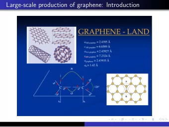
Graphene • An allotrope of carbon • Consist of a single layer of carbon atoms arranged in a hexagonal lattice • Exceptional conductivity, mechanical strength, and thermal stability
Graphene synthesis • Graphene first deposited on copper substrates using chemical vapour deposition method (CVD method) • Then transferred onto desired substrates Copper substrates
Limitations of Graphene synthesis 1. Transferring process Degradation of the transferred graphene Direct growth on desired substrate much preferable
Limitations of Graphene synthesis 2. Requires high temperatures >1000 ̊ C Does not allow graphene to be grown on the substrates required in wearable and flexible electronics As they are damaged at high temperatures.
Plasma assisted CVD • The carbon precursor will be exposed to radio frequency (RF) plasma before deposition. Dissociate carbon precursor and promote the graphene growth even at very low temperature
Gas sensing • High surface to volume ratio • Remarkable conductivity Promising for gas molecule sensing
Photo detection - Graphene/Silicon interface • The silicon opens a band gap in graphene • Enables it to detect light • Effect of hydrogen functionalisation on the graphene/silicon interface was also explored Graphene Silicon
Aim: To synthesize graphene at low temperatures with the help of plasma and investigates its use as a hydrogen gas sensor and photodetector.
CVD method used to grow graphene
Transferring • Used the PMMA assisted wet transfer method • Transferred onto on to PET and silicon
Raman spectroscopy • Confirm the existence and quality of the graphene grown • shows the presence of impurities (if there are any)
Photocurrent measurements • Taken by measuring the current following through the sample when a bias voltage is applied to it
IV IV measurements • A current was allowed to flow through the graphene and the voltage through the graphene was measured. • IV graph was obtained. • By Ohm’s law, the resistance of the graphene can be calculated from the gradient of that graph.
Results Flow rate was kept at 10 sccm for CH 4 and 2 sccm for H 2. Sample Temperature Duration of Power of plasma grown/ ̊ C growth/ min used / w A 1015 15 none B 800 15 100
Results from Raman Spectroscopy • Sample A shows the presence 8500 D peak G peak 2D peak 8000 of “2D” band, which is the 7500 Sample A 7000 characteristic peak of 6500 Intensity (a.u.) 6000 graphene. 5500 5000 successfully grown graphene 4500 4000 with plasma at 800 C 3500 3000 Sample B 2500 2000 1500 1000 1500 2000 2500 3000 -1 ) Raman Shift (cm
Results from IV IV measurements • Resistance of plasma 20 assisted CVD graphene = 22kΩ 10 Voltage (V) • Resistance of normal 0 CVD graphene -10 = 10kΩ A -20 B -30 -0.0010 -0.0005 0.0000 0.0005 0.0010 Current (mA)
Results from IV IV measurements • Could be because plasma assisted CVD Conduction band process caused the fermi level to shift Band gap to form display characteristics of Valence band doped graphene, and be more insulating
Results after exposure to hydrogen pla lasma • Resistance of graphene increased • After 20 mins, resistance saturates Exposure to hydrogen plasma reduces the conductivity of the graphene.
Results after exposure to hydrogen pla lasma • As the hydrogen plasma reacts with the graphene • Hydrogenated graphene is formed Which means that the carbon bonds are in a sp 3 configuration, as opposed to • graphene's sp 2 configuration less delocalized electrons to conduct electricity Thus graphene became more insulating Legend: After exposure to Carbon atom H 2 plasma Electron Hydrogen atom Bond
Results after heating • Resistance of the graphene went nearly back to the original resistance before hydrogenation. • This could be because when heated, the bound hydrogen atoms thermally desorbs, • Restoring the graphene to its pristine stage This shows that plasma assisted CVD graphene is suitable to be used as a gas sensor for hydrogen gas.
Graphene on sil ilicon • This graph shows telling characteristics of a diode. 25 20 • This could be because between graphene 15 and silicon there is a potential gradient 10 • With enough energy, electrons will spill from Voltage (V) 5 the graphene in to silicon. 0 • The transferred electron cannot move back to -5 the graphene due to the electron not having -10 enough energy to cross the Schottky barrier. -15 • This causes the graphene to exhibit p type -0.0010 -0.0005 0.0000 0.0005 0.0010 doping, be more insulating as well as exhibit Current (mA) properties of a diode.
Graphene on sil ilicon • The photo current increase when light -5 3.0x10 is shone Without exposure to hydrogen plasma -5 2.5x10 After 5 min of exposure • This could be because when light is Photocurrent (A) After 10 min of exposure -5 2.0x10 shining on the graphene/silicon interface, the electrons absorb energy -5 1.5x10 from light, -5 1.0x10 • Causing them to dislodge from the -6 5.0x10 graphene and become free electrons • Improving the conductivity of 0.0 graphene. 20 40 60 80 100 120 Time (s)
Graphene on sil ilicon • After exposure to hydrogen plasma photocurrent increase increases. -5 3.0x10 Without exposure to hydrogen plasma • This could be due to pronounced -5 2.5x10 After 5 min of exposure electron-hole separation efficiency and Photocurrent (A) After 10 min of exposure -5 2.0x10 low electron hole recombination. -5 1.5x10 Graphene/ silicon interface can be -5 1.0x10 used as photodetector and exposure to hydrogen plasma increases its sensitivity -6 5.0x10 to light 0.0 20 40 60 80 100 120 Time (s)
Conclusions • Graphene was successfully grown with plasma at 800 C. • Plasma assisted CVD graphene is shown to be suitable to be used as a gas sensor for hydrogen gas. • A graphene/silicon-based photodiode was also successfully demonstrated • The sensitivity of the graphene/silicon photodiode improves with hydrogenation of graphene.
Thank you
Recommend
More recommend
Explore More Topics
Stay informed with curated content and fresh updates.
