Electronic transport as a tool to study the microscopic structure of - PowerPoint PPT Presentation
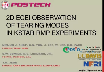
Electronic transport as a tool to study the microscopic structure of a density-wave state Pavel Grigoriev L. D. Landau Institute for Theoretical Physics, Chernogolovka, Russia What information about DW can be obtained from simple electronic
Electronic transport as a tool to study the microscopic structure of a density-wave state Pavel Grigoriev L. D. Landau Institute for Theoretical Physics, Chernogolovka, Russia What information about DW can be obtained from simple electronic transport measurements? Puzzling experimental data and their explanation will be presented Part 1: temperature dependence of conductivity anisotropy Part 2: huge maximum of longitudinal interlayer magnetoresistance and the phase inversion of magnetic quantum oscillations (SdH)
2 Motivation Why magnetoresistance studies are important? There are only few methods to study electronic dispersion E(p) and Fermi surface (FS) geometry in metals, including strongly-correlated systems with competing orders. These methods include: 2 e v v T 1. Conductivity tensor gives ij i j ij FS only general information about anisotropy of E(p) and about phase transitions with lowering temperature. 2. Band-structure calculations (rough, not always reliable) 3. ARPES (Angle resolved photoemission spectroscopy) Drawbacks: (i) Not always available; (ii) Only surface electrons participate; (iii) low resolution >10meV. 4. Magnetotransport: angular and field dependence of MR, including magnetic quantum oscillations (powerful tool, useful both alone or as complementary to ARPES).
3 Motivation ARPES (A ARPES (Ang ngle r le res esolv olved ed ph photo otoem emission ission sp spec ectr tros osco copy) y) Main idea: E k = kinetic energy of the outgoing electron — can be measured. incoming photon energy - known from experiment, φ = known electron work function. Angle resolution of photoemitted electrons gives their momentum. Rev.Mod.Phys. 75, 473 (2003) The photocurrent intensity is proportional to a one-particle spectral function multiplied by the Fermi function: Therefore can find out information about E(k) Drawbacks: 1) Often unavailable; 2) Only surface electrons participate.
4 Motivation ARPES data and Fermi-surface shape The Fermi surface of near optimally doped (a) integrated intensity map (10-meV window centered at EF ) for Bi2212 at 300 K obtained with 21.2-eV photons (HeI line); (b),(c) superposition of the main Fermi surface (thick lines) and of its (p,p) translation (thin dashed lines) due to backfolded shadow bands; (d) Fermi surface calculated by Massidda et al. (1988). Drawba Dr awback 3: k 3: Lo Low r w reso esolution lution => amb => ambiguo iguous us inte interpr pret etation tion
5 Motivation Phase diagram of high-Tc cuprate SC. Importance of magnetoresistance studies. Nd 2-x Ce x CuO 4 Theory predicts shift of the QPT point in (NCCO) SC phase? How strong is this shift? Reconstructed FS: Original FS: T. Helm, M. Kartsovnik et al., S h 1.1% of S BZ ; PRL 103, 157002 D 0.15 64 meV; (2009) n = 0.17 D 0.16 36 meV S h = 41.5% of S BZ n = 0.15 and 0.16
6 Introduction Peierls instability and density wave If the electron dispersion satisfies nesting condition: (at (a t least least on some on some fi finite nite pa part of t of ( k ) ( k Q ) 0 the F th e Fer ermi mi sur surfac ace e in in met metals), als), N the susceptibility (Q N ) diverges. Then at low temperature any e-e interaction leads to a new many-body state, which is a charge- or spin-density wave (CDW or SDW). Main features of CDW/SDW: A gap in electron spectrum appears in CDW or SDW state. If this gap covers the whole FS, the metal becomes an insulator. The modulation of charge or spin electron density can be detected by x-ray for CDW and by NMR, neutron or muon scattering for SDW.
7 Introduction Geometrical interpretation of nesting condition Quasi-1D metals Quasi-2D metals ( k ) v (| k | k ) 2 t cos( k b ) hidden1D anisotropy F F y y satisfies nesting condition: ( k ) ( k Q ) 0 N Fermi . surface Q 2 k b , / with N F k y k x 3D metals partial Fermi nesting surface Nesting vector Q N
8 Introduction Peierls transition in 1D metals Electronic susceptibility as Electron density and lattice function wave vector and distortion for half-filled band temperature G. Gruener, Density waves in Solids , 1994
9 Introduction Charge- and spin-density wave Charge-density wave Spin-density wave Density modulations for two spin Density modulations for two spin components in SDW: components in CDW: D D ( x ) cos( Qx ) ( x ) x Qx ( ) cos( ) 0 0 D x Qx ( ) cos( ) Spin-up electron x x 0 ( ) ( ) ( x density ) C x x Total charge density is modulated Total charge density is constant: D x x x const ( ) ( ) ( ) : ( x ) ( x ) ( x ) 2 cos Q x C C 0 0 Total spin density is constant Total spin density has modulation . 2 D ( x ) ( x ) ( x ) 0 . x x x Q x ( ) ( ) ( ) cos S S 0
10 Introduction STM images of CDW Real space Fourier (k-space) STM images of the ( b, c) plane of NbSe3, scanned area 20 × 20 nm2. (a)T = 77 K. Vbias = +100 mV, I = 1 nA. (b) Fourier transform of the STM image. (c) T = 5K, Vbias = +200mV, I = 150 pA T = 77 K T he Q2 CDW appears (d) 2D Fourier transform of the STM image shown in (c). NbSe 3 CDW transition temperatures : T P1 = 144K and T P2 = 59K T = 5K CDW can be visually observed via STM as intensity modulation. C. Brun et al., PRB 80, 045423 (2009) also in P. Monceau, Adv. Phys. 61, 325 (2012)
11 Introduction CDW / SDW band structure E Electron Hamiltonian in the mean field approximation: 2 D ˆ ˆ D H ( k ) a ( k ) a ( k ) a ( k Q ) a ( k ) . Q Q k k k x ˆ D g a ( k ' Q ) a ( k ' ) The order parameter ' ' k ' ' Energy band diagrams is a number for CDW, and a spin operator . ˆ D D for SDW: ˆ l Empty Q 0 E states Energy spectrum in the CDW /SDW state 2 D 2 k k Q k k Q ( ) ( ) ( ) ( ) D 2 N N E k . 2 2 k k Q 0 ( ) ( ) . Perfect nesting condition: N D k y ( k ) ( k Q ) Partial nesting condition: for some k N
12 Introduction Typical resistivity behavior during the CDW/SDW phase transition 1. Total FS is gapped => 2. FS is partially gapped => exponential (insulating) temperature dependence of R is temperature dependence metallic with jump at T p and different slope in a CDW state. G. Gruener, Density waves in Solids , 1994
13 Part 1 Spontaneous breaking of isotropy observed in the electronic transport of rare-earth tritellurides or In-plane conductivity anisotropy caused by the charge density wave state in rare-earth tritellurides and how it can be used to reveal the microscopic structure of the DW state A.A. Sinchenko, P.D. Grigoriev, P. Lejay, P. Monceau, Phys. Rev. Lett. 112, 036601 (2014)
14 Experimental Anisotropy of in-plane conductivity in RTe 3 data: Experimental observations: Above CDW transition temperature T p1 (=336K for TbTe 3 ) the in-plane conductivity is isotropic: c = a Below T p1 the in-plane conductivity is anisotropic: a > c Resistivity increases stronger in the direction a Q N || c , which expels domain-wall CDW scenario Notations: a and c along conducting layers c=y b=z a=x
15 Introduction Crystal structure of rare-earth tritellurides RTe 3 F. Schmitt et al., New Journal of Physics 13, 063022 (2011)
16 Experimental data: ARPES data on momentum dependence of CDW energy gap in TbTe 3 F. Schmitt et al., New Journal of Physics 13, 063022 (2011)
17 Experimental data: Momentum dependence of CDW energy gap (determined from ARPES) V. Brouet et al., Phys. Rev. B 77, 235104 (2008)
18 Explanation Electron dispersion and velocity. Effect of momentum asymmetry of CDW gap. The momentum dependence of Electron dispersion without electron velocity without CDW: CDW determined from band- structure calculations: Fermi surface 2 V x => 2 V y where gap -k x0 k x0 momentum asymmetry Electron conductivity: of CDW gap: ! CDW energy gap removes the electron states from FS parts with 2 , thus breaking larger component V x the x-y isotropy of conductivity.
19 Results (1) 1. The anisotropy ratio depends strongly on t / t || in the electron dispersion without CDW. This can help to extract t from experiment. For RTe 3 where R=Tb,Dy,Ho, with and the calculated maximum anisotropy ratio (at T=0) agrees with experiment, where this ratio 2 experimental data
20 Calculation of the temperature dependence of resistivity Electronic conductivity in the -approximation: CDW energy gap: For TbTe 3 Electron dispersion in the CDW state Electron velocity: Conductivity components where is the electron dispersion without CDW
Recommend
More recommend
Explore More Topics
Stay informed with curated content and fresh updates.

