EE 457 Unit 2b Fast Adders Carry-Lookahead Adders (Carry-Lookahead - PowerPoint PPT Presentation
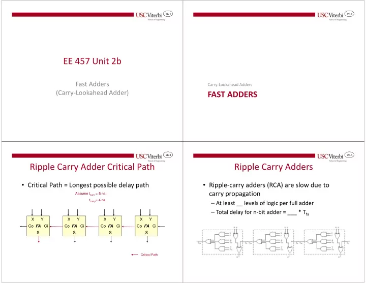
2b.1 2b.2 EE 457 Unit 2b Fast Adders Carry-Lookahead Adders (Carry-Lookahead Adder) FAST ADDERS 2b.3 2b.4 Ripple Carry Adder Critical Path Ripple Carry Adders Critical Path = Longest possible delay path Ripple-carry adders (RCA)
2b.1 2b.2 EE 457 Unit 2b Fast Adders Carry-Lookahead Adders (Carry-Lookahead Adder) FAST ADDERS 2b.3 2b.4 Ripple Carry Adder Critical Path Ripple Carry Adders • Critical Path = Longest possible delay path • Ripple-carry adders (RCA) are slow due to carry propagation Assume t sum = 5 ns, t carry = 4 ns – At least __ levels of logic per full adder – Total delay for n-bit adder = ___ * T fa X Y X Y X Y X Y Co FA Ci Co FA Ci Co FA Ci Co FA Ci S S S S Critical Path
2b.5 2b.6 Fast Adders Fast Adders • Recall that any logic function can be implemented as a • To produce multiple carries in parallel, let us define some new ____________ implementation signals for each column of addition that indicate information – SOP (AND-OR / NAND-NAND) implementation about the carry-out regardless of carry-in: – POS (OR-AND / NOR-NOR) implementation – g i = ____________: This column will generate a carry-out whether or not ______________________ • Rather than waiting for the previous carry, g i is true when A i and B i is 1 => g i = A i • B i [C i+1 = ___________] can we compute the carry as a – p i = _____________: This column will propagate a carry-in (if there is one) to the carry-out. function of just the inputs p i is true when A i or B i is 1 => p i = A i + B i – C i+1 = f(X i ,X i-1 ,…X 0 ,Y i ,Y i-1 ,…Y 0 ) • Using these signals, we can define the carry-out (c i+1 ) as: – This requires gates with many inputs which is infeasible in c i+1 = __________ modern technologies above 4 or 5 inputs – But, we can try to use this idea of generating multiple _______________ by looking at many inputs 2b.7 2b.8 Carry Lookahead Analogy Carry Lookahead Logic • Consider the carry-chain like a long tube broken into • Define each carry in terms of p i , g i and the segments. Each segment is controlled by a valve initial carry-in (c 0 ) and not in terms of ____ (propagate signal) and can insert a fluid into that __________________________________ segment (generate signal) • c1 = g 0 + p 0 c 0 • The carry-out of the diagram below will be true if g1 • c2 = g 1 + p 1 c 1 = __________________ is true or p1 is true and g0 is true, or p1, p0 and c1 is true • c3 = • c4 =
2b.9 2b.10 4-Bit CLA Carry Lookahead Adder • At this point we should probably stop as we have a _______ gate in our • Use carry-lookahead logic equation to generate all the carries • Let’s take our logic and build a 4-bit carry lookahead adder (CLA) in one shot and then create the sum a3 b3 a2 b2 a1 b1 a0 b0 c0 • Example 4-bit CLA shown Delay to produce s2 • Delay for pi,gi = ____ below • Delay to produce c2 = ___ • Delay to produce s2 = ___ s3 s2 s1 s0 = ___ gates c4 p3 g3 c3 p2 g2 c2 p1 g1 c1 p0 g0 CLL c0 (Compare to 8 gate delays for C4 P G RCA) Is S3 produced later than S2? Is C3 the last signal produced? 2b.11 2b.12 16-Bit CLA 16-bit CLA Closer Look • Each 4-bit CLA only propagates its overall carry-in if each of the 4 columns propagates: • At this point we should probably stop as we have a 5-input gate in our P0 = p3 • p2 • p1 • p0 – equation – P1 = p7 • p6 • p5 • p4 – P2 = p11 • p10 • p9 • p8 A[15:12] B[15:12] A[11:8] B[11:8] A[7:4] B[7:4] A[3:0] B[3:0] C0 – P3 = p15 • p14 • p13 • p12 • Each 4-bit CLA generates a carry if any column generates and the more significant columns C12 C8 C4 PG PG PG PG propagate – G0 = g3 + (p3 • g2) + (p3 • p2 • g1)+(p3 • p2 • p1 • g0) C16 S[15:12] S[11:8] S[7:4] S[3:0] – … 16-bit RCA Delay = _____ = ____ gate delays – G3 = g15 + (p15 • g14) + (p15 • p14 • g13)+(p15 • p14 • p13 • g12) Delay of the above adder design = __________ = ___ gates • The higher order CLL logic (producing C4,C8,C12,C16) then is realized as: Let us improve by looking ahead at a higher level to produce – (C4) =>C1 = G0 + (P0 • c0) C16, C12, C8, C4 in _______________ – … – (C16) => C4 = G3 + (P3 • G2) + (P3 • P2 • G1) +(P3 • P2 • P1 • G0)+ (P3 • P2 • P1 • P0 • c0) Define P and G as the overall Propagate and Generate These equations are exactly the same CLL logic we derived earlier • signals for a set of 4 bits What’s the difference P = ____________________ between the equation for G here and C4 on G = ___________________________________________ the previous slides
2b.13 2b.14 16-Bit CLA 64-Bit CLA • Understanding 16-bit CLA hierarchy… • We can reuse the same CLL logic to build a 64-bit CLA C0 C0 c63 s35 Pi,Gi c15 C60 C56 C52 C44 C40 C36 C28 C24 C20 C12 C8 C4 G CLL CLL CLL CLL P G P G P G P G G CLL CLL CLL CLL Pi*,Gi* P G P G P G P G C12 C8 C4 C32 C48 C16 Pi**,Gi** p3 g3 c3 p2 g2 c2 p1 g1 c1 p0 g0 p3 g3 c3 p2 g2 c2 p1 g1 c1 p0 g0 CLL c4 c0 CLL c0 c4 P* G* P G C16 Delay = = ___ = Delay in producing Pi,Gi = ___ = Delay in producing S63 = ___ = Delay in producing Pi,Gi = ___ = Delay in producing Pj*,Gj* Is the delay in producing s63 the same as in s35? = ___ = Delay in producing Pi*,Gi* = ___ = Delay in producing C48 = ___ = Delay in producing S2 = ___ = Delay in producing C60 = ___ = Delay in producing C4,C8,C12,C16 = ___ = Delay in producing S0 = ___ = Delay in producing C63 = ___ = Delay in producing c15 = ___ = Delay in producing S63 = ___ = Delay in producing S15 = _____ Total Delay 2b.15 2b.16 Extrapolating CLA Logic Levels Blocking factor of 2 • In the above designs we’ve assumed 5-input AND • Each A box and OR gates are reasonable allowing us to group in generates blocks of 4 – p i = a i + b i – Define b = blocking factor = number of carries produced in – g i = a i • b i parallel – s i = a i ⊕ b i • The greater the blocking factor the smaller the depth • Each B box of logic (and vice-versa) generates • This leads us to reason that the delay of a CLA is – P i = p i • p i-1 O(log b n) – G i = g i +p i • g i-1 • If we could only use 3-input gates we’d need a – c i+1 =G i + (P i • c i ) blocking factor of 2
2b.17 2b.18 Credits • Key lesson: In logic design trees are better • These slides were derived from Gandhi than chains! Puvvada’s EE 457 Class Notes
Recommend
More recommend
Explore More Topics
Stay informed with curated content and fresh updates.

