Dirac Materials A.V. Balatsky New class of materials What is the - PowerPoint PPT Presentation
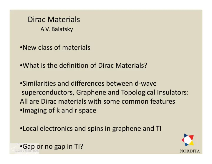
Dirac Materials A.V. Balatsky New class of materials What is the definition of Dirac Materials? Similarities and differences between d wave superconductors, Graphene and Topological Insulators: All are Dirac materials with some
Dirac Materials A.V. Balatsky • New class of materials • What is the definition of Dirac Materials? • Similarities and differences between d ‐ wave superconductors, Graphene and Topological Insulators: All are Dirac materials with some common features • Imaging of k and r space • Local electronics and spins in graphene and TI • Gap or no gap in TI?
J. X. Zhu, I. Martin, M. Salkola, T. Das, – Los Alamos D. Abergel, A. Black ‐ Schaffer Nordita H. Dahal ‐ BC T. Wehling, A. Lichtenstein, K. Scharnberg, R. Wiesendanger – U Hamburg M. Katsnelson – U Niemegen J. Fransson ‐ Uppsala D.Arovas ‐ UCSD Z. Huang – UCSD, Los Alamos Experiment: J.C. Davis group Y.Zhao, V. Brar, M. Crommie ‐ IETS L. Mattos, H. Manoharan –Kondo graphene
The Dirac Equation P. Dirac: “ The quantum theory of the electron ” (1928) with 4x4 Dirac matrices (from nobelprize.org) Describing electrons, protons, quarks,neutrinos... Nobel Price 1933 ... with peculiar physical consequences: • Spin 1/2 and Landé g=2 • Klein paradox and Zitterbewegung • Antiparticles • Spin orbit coupling
Dirac materials • Materials whose low energy electronic properties are a direct consequence of Dirac spectrum E = vk: specific heat ~T^d, penetration depth~T, optical conductivity~T^n • How do we “design” Dirac Materials? • Can be a collective state: 3He superfluid, heavy fermion, organic, high Tc superconductors, density wave states • Band structure effect – graphene, Topological states, cold atom DM, artificial DM • Not a Dirac equation (1928) T. Wehling, A Black ‐ Schaffer and A. V. Balatsky, Dirac Materials, Adv Phys, p1 v 90 (2014)
Dirac materials vs metals Metals Dirac materials (3He included) empty FS occupied E = v(k ‐ k_F) E = vk, k_F = 0 Defining feature: Dimensionality of zero energy states in one less( at least) In the Dirac materials. Fewer excitations at low T. Better control of response and less dissipation. Important for future energy and device applications.
Why Dirac materials: path to control of electronic states Tunability and control Bi2Se3 1 With B, E fields 2 with doping and functionalization Fe or Sn 3 with quantum size control: films, ribbons
R ‐ space vs K ‐ space probes of Dirac Materials Extended probes (k space) time Local probes (r space) time Magnetotrasport, thermal STM, spin imaging with Kerr conductivity Theory Guidance for search of new states Ab initio, functionalization, How protected are topological states ) Y. Xia et al. , T. Hanaguri, A. Kapitulink, H. Manoharan Nature Phys. 5 , 398 (2009) S.C. Zhang et al RMP, Nov (2011) V. Madhavan, A. Yazdani A.C. Neto et al, RMP (2010) A.V. Balatsky et al, v 78, 373 (2006)
Universal response to defects. Why Impurities? • Why local signatures and impurities? – Scientific interests : applications rely heavily on functionalization – Observation possible by Scanning Tunneling Spectroscopy (STS) – Engineered electronic states due to imp bands – Microchips at one atom at time approach ~ 100 impurity atoms/transistor mean lifetime pictures will break down. – Suggested Quantum Computation operations involve deliberate local perturbations
Local impurity resonances in d ‐ wave superconductors
d ‐ wave Superconductor:Impurity Resonances LDOS Image at On-site potential On-site LDOS for impurity-state U>0 Cross shaped j i F 2 9 0 9 3 0 . 6 6 5 4 1 0 9 5 1 . 9 9 j state - E E 1 1 2.5 typical region 2 N U ln 8 N U on center of Zn atom 0 F F Differential Conductance (nS) 2.0 Rev. Mod Phys, 78 , p 373, (2006) 1.5 1.0 0.5 0.0 -100 -50 0 50 100 Sam ple Bias (m V)
Impurity states in ANY Dirac point materials
Impurity states in ANY Dirac point materials
Impurity states in ANY Dirac point materials 1/U_1
Impurity states in ANY Dirac point materials 1/U_1 1/U_2
Impurity states in ANY Dirac point materials
Local impurity resonances in Dirac Materials: Graphene
Real space signatures I T. Wehling et. al., PRB 75, 125425 (2007), Peres, A.C Neto, Guinea, Falko r ‐ dependent LDOS at imp. resonance E imp =0.1eV
M.M. Udega etal, PRL104, 096804 (2010)
Universal response to local defects Hypothesis: ANY Dirac material has similar resonances Graphene D ‐ Wave SC 2.5 typical region on center of Zn atom Differential Conductance (nS) 2.0 1.5 1.0 0.5 0.0 -100 -50 0 50 100 Sam ple Bias (m V)
Local impurity resonances in Topological Insulators, probe of stability Hanaguri etal, PRB 2010, cond mat 1003.0100
Impurity resonances in Dirac Materials: Topological Insulators, probe of suppressed back scattering Hanaguri etal, PRB82, 081305(2010); Gomes et al , arXiv:0909.0921 Cheng, et al, PRL 105, 081305(2010). (2009)
Resonance as seen in STM Z. Alpichev et al, PRL 108,206102,(2012) Sessi et al. NATURE COMM | DOI: 10.1038/ncomms6349, (2014)
ARPES on magnetically doped TI and on films H k S z z 2 2 E k S z Fully gapped spectrum
At B=0 at Dirac point now there should Be a true gap. The data show finite LDOS. Gap or no gap for Cr doped sample.
Gap in FM ordered TI seen in STM
Robust conventional IQHE has mobility gaps, not real gaps
Gas vs Mobility gap in (A) QHE Anomalous QHE that Conventional IQHE does not require a full gap either
Z. Alpichev et al, PRL 108,206102,(2012) No gap at zero field
Competing trends due to magnetic scattering Low energy resonance Magnetic scattering • Every impurity (magnetic Gap in Dirac spectrum and nonmagnetic) will • Dirac fermion acquire a produce imp resonances mass due to spin Science 329, 659 (2010); inside Dirac cone = Y. L. Chen, et al. backscattering H k S z z 2 2 E k S z N(E) + = True answer is combination of both effects Biswas, AVB PR B 81 , p233405 (2010), A Black Schaffer et at, arXiv:1502.06403
Filling of Magnetic Impurity Induced Gap in Topological Insulators by Potential Scattering arXiv:1502.06403 , A. M. Black-Schaffer, A. V. Balatsky, J. Fransson E E_f Science 329, 659 (2010); Y. L. Chen, et al.
Artificial Dirac Materials Nanoscale functionalization in Graphene physics Nanoassembled artificial graphene Manoharan group, Nature 483, p 306, 2012 doi:10.1038/nature10941
Universal response of Dirac materials to local perturbations Graphene 2.5 D ‐ Wave SC typical region on center of Zn atom Differential Conductance (nS) 2.0 1.5 1.0 0.5 0.0 -100 -50 0 50 100 1.2 Sam ple Bias (m V) 1.0 TI dI/dV (arb. unit) 0.8 0.6 0.4 0.2 0.0 -600 -400 -200 0 Sample bias (mV)
Conclusion • Dirac materials is a class • Convergence in multiple materials ‐ > class. • Defects as test of stability of Topological states • The future is even more exciting with designed materials coming. • New imaging to capture exciting new phenomena in quantum materials
Recommend
More recommend
Explore More Topics
Stay informed with curated content and fresh updates.
