CPU Organization Scope We will build a CPU to implement our subset - PowerPoint PPT Presentation
5.1 5.2 CPU Organization Scope We will build a CPU to implement our subset of the MIPS ISA Memory Reference Instructions: Load Word (LW) EE 457 Unit 5 Store Word (SW) Arithmetic and Logic Instructions: ADD, SUB, AND, OR,
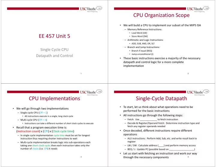
5.1 5.2 CPU Organization Scope • We will build a CPU to implement our subset of the MIPS ISA – Memory Reference Instructions: • Load Word (LW) EE 457 Unit 5 • Store Word (SW) – Arithmetic and Logic Instructions: • ADD, SUB, AND, OR, SLT – Branch and Jump Instructions: Single Cycle CPU • Branch if equal (BEQ) • Jump unconditional (J) Datapath and Control • These basic instructions exercise a majority of the necessary datapath and control logic for a more complete implementation 1 2 5.3 5.4 CPU Implementations Single-Cycle Datapath • To start, let us think about what operations need to be • We will go through two implementations performed for the basic instructions – Single-cycle CPU (CPI = 1) • All instructions go through the following steps: • All instructions execute in a single, long clock cycle – Fetch: Use _____________ to fetch instruction – Multi-cycle CPU (CPI = n) – Decode & Register/Operand Fetch: Determine instruction type and • Instructions can take a different number of short clock cycles to execute fetch any register operands needed • Recall that a program execution time is: • Once decoded, different instructions require different (Instruction count) x (CPI) x (Clock cycle time) operations – In single-cycle implementation cycle time must be set for longest instruction thus requiring shorter instructions to wait – ALU instructions: Perform Add, Sub, etc. and write result back to register – Multi-cycle implementation breaks logic into sub-operations each taking one short clock cycle; then each instruction takes only the – LW / SW: Calculate address (____) and perform memory access number of clocks (i.e. CPI) it needs – BEQ / J: Update PC (possible based on ___________________) • Let us start with fetching an instruction and work our way through the necessary components 3 4
5.5 5.6 Instruction Ordering Fetch • Identify which components each instruction type would use • Address in PC is used to fetch instruction while it is also and in what order: ALU-Type, LW, SW, BEQ incremented by 4 to point to the next instruction • Remember, the PC doesn’t update until the end of the clock cycle / beginning of next cycle Zero PC General Addr. Data Addr. Data • Mux provides a path for branch target addresses ALU Purpose Res. Registers I-Cache / I-MEM D-Cache / D-MEM Fetch branch target LW ALU-Type SW BEQ 4 0x0040001c (LW $5,40($7) A (ADD $5,$6,$7) (SW $5,40($7) (BEQ $2,$3,disp) + PC+4 B 0x00400018 opcode rs rt rd shamt func 0x00400018 Addr. 000000 01001 01010 10000 00000 100000 0 Instruc. 1 0x012a8020 I-Cache ADD $16,$9,$10 PC 6 5.7 5.8 Decode Datapath for ALU instruction Opcode and func. field are decoded to produce other control signals • • ALU takes inputs from register file and • Execution of an ALU instruction (ADD $3,$1,$2) requires reading 2 register values and writing the result to a third performs the add, sub, and, or, slt, operations • REGWrite is an enable signal indicating the write data should be written to • Result is written back to dest. register the specified register Control Control Signals opcode Logic 000000 00001 00010 Read Read Value of $1 1 Reg. 1 # data 1 Read Reg. 1 # rs Read ALUop Read 2 Value of $2 Reg. 2 # Read data 2 Instruc. word Reg. 2 # Instruction Word rt Write Read $1 value 3 Reg. # Write data 1 Register File is the collection of GPR’s. Our register ADD $3,$1,$2 Zero Reg. # ALU ADD $3,$1,$2 00011 file has 3 “______” (ability to concurrently read or Write $2 value Res. rd Read Sum Data write a register). To see why we need 3, consider Write data 2 Register File Data an “ADD $3,$1,$2”. We need 2 ___________ to shamt 00000 Register File read two operands (i.e. $1 + $2) and 1 ______ for the result ($3) 100000 func 7 8 CLK REGWrite Result from add
5.9 5.10 Memory Access Datapath Branch Datapath • BEQ requires… • Operands are read from register file while offset is sign extended – ALU for comparison (examine ‘zero’ output) • ALU calculates __________________ – Sign extension unit for branch offset • Memory access is performed If LW, ____________________ – Adder to add PC and offset • • Need a separate adder since ALU is used to perform comparison LW $4,0xfff8($1) SW $3,0x1a($1) PC+4 (incremented PC) Adder 1 Read 1 Sum Branch Target Read Reg. 1 # Shift Address to PC Reg. 1 # ADD Left 2 Read Read 3 Read Reg. 2 # Reg. 1 # $1 value Reg. 2 # byte offset Read ALUop $1 value 4 Read Write data 1 Zero Read Instruc. word Write data 1 Zero Reg. # ALU Reg. 2 # Res. Reg. # ALU Read $1 value Addr. Read Read Res. Write Sum Addr. Write BEQ $1,$2,offset data 1 Read data 2 ZERO Data Zero Write Sum Data Read Reg. # ALU data 2 Data Read Data $2 value Res. Read Sum Register File Data Write Write Register File data 2 $3 value Data Write Data Data Sign Register File Write Data D-Cache Sign Extend 32 0xffff fff8 D-Cache Extend word offset extended word offset 32 0x0000001a 9 10 Sign Extend 5.11 5.12 Fetch Datapath Question 1 Fetch Datapath Question 2 • Can the adder used to increment the PC be an ALU and be • Do we need the “Write” enable signal on the PC register for used/shared for ALU instructions like ADD/SUB/etc. our single-cycle CPU? – In a single-cycle CPU, _______________________________ – In the single-cycle CPU, ______________________________ _________________________________________________ “Next” PC = PC + 4 “Next” PC = PC + 4 4 A 4 A + + S S B B CLK CLK Addr. Data Addr. Data PC PC Instruction Word Instruction Word Current PC / Current PC / Read Address Read Address I-Cache / I-MEM I-Cache / I-MEM Write Write 11 12
5.13 5.14 RegFile Question 1 RegFile Question 2 • Why do we need the write enable signal, REGWrite? • Can write to registers be level sensitive or does it have to be edge-sensitive? Control Control Control Signals Control Signals Logic Logic opcode 000000 opcode 000000 Read Read Read Read Value of $1 Value of $1 Reg. 1 # data 1 Reg. 1 # data 1 00001 00010 00011 00001 00010 00011 5 5 rs rs Read Read Read Read Value of $2 Reg. 2 # Reg. 2 # Value of $2 data 2 data 2 5 5 Instruction Word Instruction Word rt rt Write Write Reg. # Reg. # 5 5 ex. ALU instruc. ex. ALU instruc. Write Write rd rd Data Data Register File Register File shamt 00000 100000 shamt 00000 100000 func func 13 14 CLK REGWrite CLK REGWrite Result from add Result from add 5.15 5.16 RegFile Question 3 Sign Extension Unit • Since we need a write enable, do we need read enables (i.e. • In a ‘LW’ or ‘SW’ instructions with RE1, RE2) their base register + offset format, the instruction only contains the offset as a 16-bit value – Example: LW $4,-8($1) offset = 0xfff8 0xfffffff8 Sign – Machine Code: 0x8c24fff8 Read Reg. 1 # Operand A Extend Read data 1 16 32 value 5 RE1 • -8 = 0xfff8 Operand B Read data 2 Read Reg. 2 # value • The 16-bit offset must be extended 5 RE2 to 32-bits before being added to base Write Reg. # 5 register Write Data Register File LW $4,0xfff8($1) 100011 00001 00100 1111 1111 1111 1000 15 16 CLK REGWrite opcode rs rt offset Result from add
5.17 5.18 Sign Extension Questions Data Memory Questions • Do we need separate instruction and data • What logic is inside a sign-extension unit? memory or can we just use one (i.e. most – How do we sign extend a number? personal computers only have one large set MemRead – Do you need a shift register? of RAM)? Read • Do we need separate read/write address Read Addr. inputs or can we have just one address input 16-bit offset b 15 b 14 b 13 … b 0 Read Data used for both operations? Write Addr. • Can we do away with the “read” control Write Data Write signal (similar to how we did away with read enables for register file)? MemWrite b 15 … b 15 b 15 b 14 b 13 … b 0 32-bit sign-extended output 17 18 5.19 5.20 Branch Datapath Question Combining Datapaths • Is it okay to start adding branch offset even before • Now we will take the datapaths for each instruction determining whether the branch is taken or not? type and try to combine them into one • Anywhere we have multiple options for a certain input we can use a mux to select the appropriate value for the given instruction PC+4 (incremented PC) Adder Branch Target Sum • Select bits must be generated to control the mux Shift Address to PC 1 Left 2 Read Reg. 1 # ALUop 2 Read Instruc. word Reg. 2 # Read $1 value Write data 1 BEQ $1,$2,offset ZERO (To control logic) Zero Reg. # ALU $2 value Res. Read Sum Write data 2 Data Register File word offset extended word offset Sign 19 20 Extend
Recommend
More recommend
Explore More Topics
Stay informed with curated content and fresh updates.


