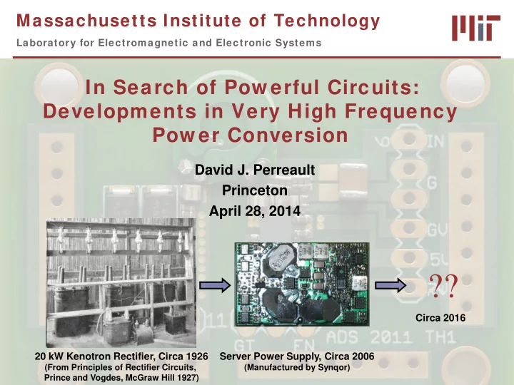
?? Circa 2016 20 kW Kenotron Rectifier, Circa 1926 Server Power - PowerPoint PPT Presentation
Massachusetts Institute of Technology Laboratory for Electromagnetic and Electronic Systems In Search of Pow erful Circuits: Developments in Very High Frequency Pow er Conversion David J. Perreault Princeton April 28, 2014 ?? Circa 2016 20
Massachusetts Institute of Technology Laboratory for Electromagnetic and Electronic Systems In Search of Pow erful Circuits: Developments in Very High Frequency Pow er Conversion David J. Perreault Princeton April 28, 2014 ?? Circa 2016 20 kW Kenotron Rectifier, Circa 1926 Server Power Supply, Circa 2006 (From Principles of Rectifier Circuits, (Manufactured by Synqor) Prince and Vogdes, McGraw Hill 1927)
Pow er Electronics The function of power electronic circuits is the processing and control of electrical energy Modern electrical and electronic devices require power electronics Lighting, computation and communication, electromechanical systems (e.g., motors), renewable generation,… In 2005 ~ 30% of generated energy goes through power electronics; this is expected to be ~ 80% by 2030 (ORNL 2005) Power electronic circuitry is often a major factor determining system size, functionality, performance and efficiency LED lightbulb and driver Lighting, Power supplies Distributed renewables Microinverter for photovoltaic systems Inverter for Prius HEV (Modified from Tolbert et al, “ Power Electronics for Distributed Energy Systems and Transmission and Distribution Applications, ” ORNL 2005)
Structure of Pow er Electronic Systems Control Input Filter Power Stage Output Filter Power processing with (ideally) lossless components Switches, inductors, capacitors, transformers,… Ancillary elements Control, heat sinking, filtering… System operates cyclically Draw some energy (switches) Store in energy storage (L’s, C’s) Transform Transfer to output Often specified to operate over wide voltage, current and power ranges
Passive Components Dominate Passive components dominate the size of power electronics Also limit cost, reliability, bandwidth,… A 25 W Line Connected LED Driver A Voltage Regulator Module for a computer
Motivations for Frequency Increases Commercial Goals LED Driver 100 kHz Miniaturization 21 W Integration 85% eff 4.8 W/in 3 Increased performance (bandwidth…) Passive energy storage components (especially magnetics) are the dominant constraint Energy storage requirements vary inversely with frequency: C,L proportional to f -1 Volume can be scaled down with frequency But, often scales down slowly with frequency Magnetic core materials especially impact frequency scaling Integration / batch fabrication of passives imposes further challenges Perreault, et. al., “Opportunities and Challenges in Very High Frequency Power Conversion,” APEC 2009
Sw itching Frequency Limitations Loss mechanisms in power electronics limit switching frequencies Relative importance of different losses depends on power, voltage Gating loss ( ∝ f ) Magnetics loss ( ∝ f k ) Switching loss ( ∝ f ) V SW (t) I SW (t) time p(t) time
Design Requirements and Device Capabilities Application requirements also impose limits on miniaturization, integration and performance e.g., line-frequency energy buffering requirement for single- phase grid interface imposes significant size constraints Large conversion ratios, wide voltage or power ranges, isolation requirements, etc., impact achievable size Devices & characteristics available in different operating regimes also greatly impact performance CMOS at low voltages (e.g., a few V) and power levels Integrated LDMOS at moderate voltages (10’s to 100’s V) at low power Discrete devices at high voltage and/or power levels Vertical Si devices GaN-on-Si devices SiC devices
Very High Frequency Pow er Conversion Objective: develop technologies to enable miniaturized, integrated power electronics operating at HF and VHF (3 – 300 MHz) To achieve miniaturization and integration: Circuit architectures, topologies and controls for HF/VHF Develop approaches that overcome loss and best leverage devices and components available for a target space Devices Optimization of integrated power devices, design of RF power IC converters, application of new devices (e.g., GaN) Passives Circuits Devices Synthesis of integrated passive structures incorporating isolation and energy storage Investigation and application of VHF-compatible magnetic materials Integration Magnetics Integration of complete systems
System Examples Low-voltage, low-power step-down conversion for battery-powered systems CMOS devices Hybrid capacitor/magnetic conversion Moderate voltage, low power Isolated dc-dc converter for power supply applications Integrated LDMOS devices PCB integrated magnetics Grid voltage, moderate power Grid-interface LED driver system Line frequency energy buffering and power factor correction Discrete GaN-on-Si devices Hybrid capacitor/magnetic conversion
Sw itching Frequency Limitations At moderate voltage levels, ALL of gating, switching and magnetics losses are important constraints on switching frequency Gating loss ( ∝ f ) Magnetics loss ( ∝ f k ) Switching loss ( ∝ f ) V SW (t) I SW (t) time p(t) time
Sw itching Frequency Solutions Minimize frequency dependent device loss, switch fast enough to eliminate/minimize magnetic materials, enable PCB integration Resonant gating ZVS Soft switching Coreless magnetics in package or substrate Sagneri, MIT, 2011 Low-permeability RF magnetic materials V D (t)
Topology Implications for VHF Conversion V in R L Inverter Rectifier Matching Inverter Transformation Rectifier Network Stage Driving high-side “flying” switches becomes impractical Circuit operation must absorb parasitics device capacitances, interconnect inductance, … Topology & device constraints impose limits Topologies are often sensitive to operating conditions Resonant gating, ZVS topologies limit control Fixed frequency and duty ratio controls become preferable
Inverter Topology: Ф 2 Inverter v DS (idealized) t Multi-resonant network shapes the switch voltage to a quasi-square wave Network nulls the second harmonic and presents high impedance near the fundamental and the third harmonic Reduces peak voltage ~ 25-40% as compared to class E Reduces sensitivity of ZVS switching to load characteristics No bulk inductance (all inductors are resonant) Small inductor size Fast transient performance for on-off control Absorbs device capacitance in a flexible manner Rivas, et. al., “A High-Frequency Resonant Inverter Topology with Low Voltage Stress,” Trans. P.E., July 2008
Isolated VHF dc-dc Topology Isolated Φ 2 inverter, resonant rectifier Single-switch resonant Inverter and resonant rectifier ZVS switching waveforms with low voltage stress Device, transformer parasitics fully absorbed provide Φ 2 inverter and rectifier tuning Fixed frequency and duty ratio enables resonant gate drive of M 1 On-off control to regulate output Transformer design critical to obtain desired tuned operation May be implemented as a planar PCB structure
Planar PCB Transformer Implementation The transformer inductance matrix is fully constrained by converter design Implement in printed circuit board Achieve characteristics by careful geometry selection Select structure that best trades size and loss Primary Sec. 1 Sec. 2 Sec. 3 Sagneri, et. al., “Transformer Synthesis for VHF Converters,” 2010 International Power Electronics Conference, June 2010
Integrated Sw itch and Controls Power applications often require integrated switches and controls in low-cost processes (e.g., LDMOS devices in a BCD process) With device layout optimization one can achieve VHF operation (30- 300 MHz) with conventional (low-cost) power processes Circuit/Device co-optimization: Optimize device layout for specific circuit waveforms Take advantage of soft switching trajectory in device design >55% loss reduction demonstrated through this method Gating Conduction Displacement Simulated Ideal Hard- Resonant Switched Trajectory Trajectory Sagneri, et. al., “Optimization of Integrated Transistors for Very High Frequency dc-dc Converters,” Trans. P.E (July 2013)
Integrated VHF Converter in BCD Process Isolated converter Half-sine resonant gate drive Integrated controls and power devices 41
Prototype Isolated Φ 2 Converter 6 W, 75 MHz isolated converter 8-12 V input, 12 V output On-off control to regulate output ZVS switching, resonant gating to achieve VHF Printed-circuit-board transformer Integrated switch, resonant driver and controls ABCD5 process
Prototype Isolated Φ 2 Converter Results ZVS Resonant waveforms over operating range Efficiency 66%-76% across voltage, load range Half-sine resonant gate driver Pgate ~ 110 mW @ 75 MHz, ~ 3x improvement over hard gating
Prototype 75 MHz Integrated Converters Isolated Φ 2 Converter Φ 2 Boost Converter 6W, 73% efficiency 14W, 85% efficiency Non-isolated (boost) variant with PCB-integrated magnetics also demonstrated Non-isolated version yields higher power, efficiency, power density Many related topology variants Pilawa-Podgurski, et. al., “Very High-Frequency Resonant Boost Converters,” Trans. P.E. June 2009
Pow er Density, Efficiency, Integration
Recommend
More recommend
Explore More Topics
Stay informed with curated content and fresh updates.
