Content Server Caching Network Client Web Server Browser Avoid - PowerPoint PPT Presentation
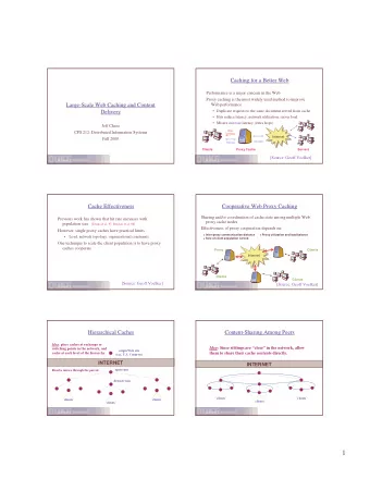
Content Server Caching Network Client Web Server Browser Avoid Network Latency Avoid Queuing Delays at Server Cache Content Locally at client Updates? Cache Content at proxies Proxy Server Client Proxy Server Content Server Proxy
Content Server Caching Network Client Web Server Browser Avoid Network Latency Avoid Queuing Delays at Server Cache Content Locally at client Updates? Cache Content at proxies Proxy Server Client Proxy Server Content Server Proxy Server 1
Caching in Device and Storage Array PORT Controller Controller I/O devices (Disk) ~2 ms - 100 ms CACHE Main Memory (DRAM) ~100 - 200 ns PORT DISK BLOCKS 2
Disk Buffer Caching PROCESSOR DISK BLOCKS I/O devices (Disk) ~2 ms - 100 ms CACHED DISK Main Memory (DRAM) ~100 - 200 ns BLOCKS Buffer Cache Why not replace slow disk with fast main memory? MAIN MEMORY Cost vs Speed (Flash SSDs?) Persistence 3
Processor Caching Main Memory DRAM: Dense, Cheaper, Slower, Needs Refresh (40ns - 100ns) Processor Cache SRAM: Expensive, Fast (5-20 ns) Integrated with the processor can operate at processor speed DRAM SRAM Cache MEMORY R L1 L2 Processor Software is aware Transparently handled by hardware 4
Cache Principle Cache holds only a small fraction of the memory blocks at any time • Keep the most valuable blocks in cache • Blocks that hold memory words being accessed • Locality Principle • Temporal Locality: • • In the near future a memory word that has been touched will be accessed again e.g. instructions in a loop, local variables in a procedure • Spatial Locality • • Locations that are close by spatially (memory addresses) will be accessed together (in close temporal proximity) e.g. sequential instruction fetches, walking an array • 5
Memory Hierarchy Review Speed (directly related to cost) R: Registers 1ns Integrated L1 Cache 1-2 ns L2 (SRAM) ~10 - 20 ns Main Memory (DRAM) ~100 - 200 ns I/O devices (Disk) ~ 2 ms - 50 ms R L1 L2 MEMORY DISK Cache and Memory Virtual Memory Controller System Performance Management Space Management 6
Memory Hierarchy Review Registers • Limited number of physical registers • Register usage managed by compiler and renaming hardware • Cache • Small high-speed memory (SRAM) • Cache hierarchy : L1 (smallest/fastest), L2, L3 optimize cost performance • Main Memory (different flavors of DRAM) • Order-of magnitude slower than cache • Accessed by memory controller using physical addresses • Disk • Large persistent storage for files • Backing store for virtual memory implementation • 7
Two-Level Memory Hierarchy L1 Cache CPU Controller CACHE DRAM Fast, small Memory Controller 8 Slow, Large capacity
Two-Level Memory Hierarchy L1 cache holds copies of some subset of the locations of main memory • Processor memory requests intercepted by cache controller • Cache Hit: • Cache holds the requested memory word (Request can be satisfied from cache) • Cache Miss: • Stall processor till request is satisfied from main memory • Copy of requested word brought from main memory into cache • Simple Analytic Model to estimate effect of stalls for memory access Memory stall cycles = Number of Misses x Miss Penalty = IC x Misses/Instruction x Miss Penalty = IC x Misses/Memory Access x Memory Accesses / Instruction x Miss Penalty = IC x Miss Rate x Memory Accesses / Instruction x Miss Penalty Miss Rate: Program memory access characteristics • Temporal and Spatial Locality • Cache Organization • Memory Accesses/Instruction: Program Characteristics • Density of LD and SD instructions (for data memory accesses) • Miss Penalty: Memory Subsystem Design • DRAM speed • Cache memory Bandwidth • Memory Parallelism and Controller • 9
Processor Cache Example Assume machine parameters: Clock Rate: 1GHz Miss penalty: 200 cycles (accessing main memory and installing in cache) Miss Rate: 1% (misses per memory access) Load/Store: make up 20% of the instructions Nominal CPI: 2 cycles (assuming 100% cache accesses) Note: Miss rate is sometimes also specified as misses per instruction, or misses per memory read, and misses per memory write Memory access/Instruction = 1 (for instruction fetch) + 0.2 (for LD or SD) = 1.2 Misses/Memory Access = Miss Rate = 1% Stall cycles/Miss = Miss penalty = 200 cycles Stall cycles / instruction = 200 x 1% x 1.2 cycles = 2.4 cycles • Actual CPI = 2 + 2.4 = 4.4 ( > 100% increase in CPI due to cache misses) • If nominal CPI was 1.0: actual CPI is 3.4 and slowdown due to cache misses • would be even greater 10 1
Processor Cache General Cache Organization: Main memory address: n+b bits Divided into blocks of 2 b consecutive bytes (Block size or Line size) N = 2 n blocks of main memory (2 n+b bytes of main memory) 2 m cache blocks (also called cache line) m << n b LSBs are used to select a byte (or word) from a block after access. n MSBs are used to access a block of the cache (cache line) n b Block Address Byte Offset B = 2 b bytes B = 2 b bytes M = 2 m Cache blocks Main N = 2 n Memory blocks Memory 11 1
Cache Example Main memory: Byte addressable memory of size 4GB = 2 32 bytes Cache size: 64KB = 2 16 bytes Block (line) size : 64 bytes = 2 6 bytes Number of memory blocks = 2 32 / 2 6 = 2 26 Number of cache blocks = 2 16 / 2 6 = 2 10 n = 26 b = 6 Block Address Byte Offset 0 63 B = 64 bytes M = 2 10 = Cache 1024 Main N = 2 26 blocks Memory blocks Memory 12 B = 64 bytes
Cache Example Main memory: Byte addressable memory of size 4GB = 2 32 bytes Cache size: 64KB = 2 16 bytes Block (line) size : 64 bytes = 2 6 bytes Number of memory blocks = 2 32 / 2 6 = 2 26 Number of cache blocks = 2 16 / 2 6 = 2 10 Is the accessed memory byte (word) in the cache? n = 26 b = 6 If so where? Block Address Byte Offset If not, where should I put it when I get it from 0 63 main memory? B = 64 bytes M = 2 10 = Cache 1024 Main N = 2 26 blocks Memory blocks Memory 13 B = 64 bytes
Fully Associative Cache Organization Fully-Associative • Set-Associative • Direct-Mapped Cache • A cache line can hold any block of main memory A block in main memory can be placed in any cache line Many- Many mapping Maintain a directory structure to indicate which block of memory currently occupies a cache block Directory structure known as the TAG Array The TAG entry for a cache stores the block number of the memory block currently in that cache location 14
Recommend
More recommend
Explore More Topics
Stay informed with curated content and fresh updates.


![1 Web Traffic Characterization Zipf Web Traffic Characterization Zipf [Breslau/Cao99] and](https://c.sambuz.com/987174/1-s.webp)
